Over the past three decades, the semiconductor industry has been able to double the functionality of silicon devices every 18 months, as predicted by Moore’s Law. However, economical and technical issues are already causing diminishing returns for dimensional scaling. To continue reducing the cost per function, the most practical solution is to move to three-dimensional integrated circuits (3D-ICs), bridging the gap between the capabilities of traditional 2D scaling and ever increasing future system requirements.
Classical dimensional scaling is facing challenges from rising on-chip interconnect delays, escalating lithography costs and layout limitations. Clearly, the growing cost of lithography has escalated the end-wafer cost, and as a result, has diminished the benefit of having more transistors. As well, the mounting interconnect delays have mostly eliminated the benefits of faster and lower power transistors.
Many have declared that the coming decade is the “3D Era” for both transistor itself, as well as for layer stacking. However, TSV connected layer stacking is proving to be expensive and is relatively limited in vertical connectivity (about 104/mm2), due to the large TSV size and the even larger keep-out-zone driven pitch. Further, foundries and IDMs have announced TSV-based 3D IC development programs, yet we are still waiting to see meaningful market adoption. At this time, only 2.5D devices – using interposers and relatively crude chip stacking, have been released to the market, and this for the narrow market of high end FPGA applications.
However, another form of 3D IC may become truly interesting – the monolithic 3D IC. In fact, all of the non-volatile memory vendors have already announced monolithic 3D NAND Flash architectures and their plans for production – see Toshiba to Build Fab for 3D NAND Flash (http://www.eetimes.com/document.asp?doc_id=1318793).
We believe that broad adoption of monolithic 3D should soon follow up. Monolithic 3D provides a 10,000 times higher vertical connectivity than TSV by means of sequential fabrication of thin (
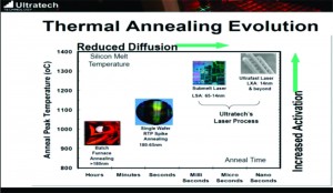
Two major semiconductor trends have advanced sufficiently to allow the industry to develop monolithic 3D IC flows using conventional semiconductor processes and materials. The first is industry’s move to fully depleted transistors (bulk or SOI, FinFet or conventional MOSFET), which utilize much less silicon volume to construct the transistor channel. The second trend is the move to shorter time-scale rapid thermal annealing. Specifically the adoption of laser annealing to achieve a sharper junction definition, as illustrated in the following chart.

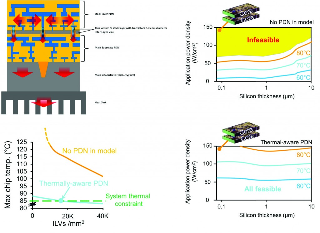
By relatively simple modifications it is now feasible to leverage the decades old ion-cut layer transfer process to obtain thin ( A known concern for 3D IC, and even more so for monolithic 3D, is removing the operational heat from active transistor layers buried inside the layer stack. A pioneering work on this was presented at the recent IEDM and been covered by the blog – Can Heat Be Removed from 3D-IC Stacks? – demonstrating that the same power network that brings power to the transistor layer stack could be used to remove the heat generated by it. This concept is illustrated below:

It reasonable to expect that 3D IC technologies will mature and help the industry compensate for the diminishing value of dimensional scaling by keeping the basic premise of Moore’s Law effective for decades to come.
Moreover, these monolithic 3D technologies would bring additional benefits that would help to propel the electronics industry further. Some of these additional benefits are:
• Significant advantages for reusing the older fab lines and design tools
• Heterogeneous Integration: Logic, Memory, Analog, RF, …
• Processing multiple layers simultaneously, offering multiples of cost improvement: 3D NAND Flash, …
• Logic redundancy, allowing 100x larger integration at good yields
• Modular Platforms: common layers combined with one or more custom layers
I will conclude by quoting Robert Gilmore, Vice President of Engineering at Qualcomm, from his invited paper at the VLSI Symposium last June in Kyoto, Japan:
“As performance mismatch between devices and interconnects increases, designs have become interconnect limited. Monolithic 3D (M3D) is an emerging integration technology that is poised to reduce the gap significantly between device and interconnect delays to extend the semiconductor roadmap beyond the 2D scaling trajectory predicted by Moore’s Law…”
Note: Some of the technology presented in this article are patented or patent pending technologies of MonolithIC 3D and others.


