EM recognizes the best products in the SMT industry. Our editors undertook a rigorous selection process of products launched in 2017, and they have selected 10 winners as the 2017 Products of the Year.
The editors evaluated products launched in 2017 based on innovative design, significant advancement in technology or application, and substantial achievement in price and performance.
Electrolube Revolutionary New 2-Part UV Cure Conformal Coating 2k850
This exciting new product combines the speed and convenience of UV cure, enabling an immediate tack-free coating, with the features and benefits of Electrolube’s revolutionary 2K conformal coating system; this innovative range combines the properties of a resin with the easy application of a coating. Once the two components are mixed, the system guarantees complete cure at room temperature within 24 hours, compared to the industry moisture cure average of about 8-14+ days.
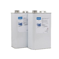 The 2K850 product offers major advantages over the first generation of single part UV cure coatings currently available. Current users of single part UV cure coating systems experiencing issues relating to their coating cracking during thermal shock, or extended moisture cure processes (or both) now have a robust alternative solution using their existing production equipment – the only additional requirement is a simple 2K fluid valve modification.
The 2K850 polyurethane system provides a much faster processing time with an advanced level of protection. The UL94V-0, IPC-CC-830C, MIL-I-46058C and IEC 61086 compliant coating features a wide operating temperature range of -40 to +130°C with excellent thermal shock performance and offers several other benefits over traditional UV cure conformal coatings. 2K850 is a tough, flexible, high performance coating, characterised by greater coating thickness (200-400μm), enhanced edge coverage and improved adhesion, hardness and scratch resistance. Ultimately, this coating provides a consistent and completely reliable chemical cure.
Electrolube’s 2K range, including 2K850 are all hydrophobic coatings, providing excellent water, moisture and condensation protection, including salt mist. This makes 2K850 an excellent choice for automotive, aerospace and other tough electronic applications exposed to harsh conditions.
Product Page Link: https://www.electrolube.com/products/conformal-coatings/2k850/2k-coatings/
Contact Details: Julia Vorley Group Marketing Manager, julia.vorley@hkw.co.uk
Indium Corporation InFORMS® Reinforced Solder Ribbon for Automated Assembly
 Indium Corporation is redefining solder with its patent-pending InFORMS solder ribbon for automated assembly.
InFORMS are reinforced solder preforms that help maintain the required bondline and promote good solder wetting. During the soldering process, the copper does not melt, ensuring that the bondline is maintained across the entire solder joint.
InFORMS solder ribbon is a composite fabrication consisting of solder and a reinforcing matrix that:
- Increases lateral strength
- Maintains bondline co-planarity
- Improves thermal cycling reliability
Product Advantages
InFORMS® offer dramatically improved handling when compared to conventional solder alloys or indium-based sheets, foils, ribbons, or large preform materials. InFORMS®® also offer increased tensile and compressive strength via the substrate materials, while retaining the unique attributes of the outer layer metal (e.g., the softness, ductility, and other advantages of indium).
Applications
InFORMS® provide engineers with an enhanced material for the development of new, or the improvement of existing, applications. They can be used in cryogenic or vacuum seals, EMI and RFI shielding, ground straps, stand-offs, thermal mismatch devices, or backplane assembly washers. While a number of metals may be used, indium metal should be considered for many applications because of its unique attributes. For example, indium readily wets glass, quartz, and glazed ceramics. When compared to conventional solders, indium-based solders significantly reduce scavenging and leaching of gold and other precious metals.
Product Details page link: www.indium.com/inform
Contact: Anita Brown, Associate Director, Marketing Communications, abrown@indium.com
JBC NASE-2B Nano Rework Station
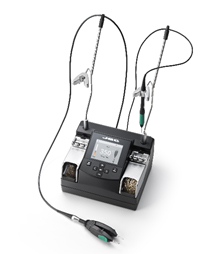 The NASE-2B best solution for repairing very small-sized components requiring the highest precision such as chips 0402, 0201, 01005, etc.
Intelligent Heat Management
When the tool is placed back on the stand, the Sleep & Hibernation features are automatically activated. This lowers the tip temperature and increases a tip’s life by more than 5.
TFT screen
The menu is intuitive and easier to use thanks to the improved interface usability.
The working screen shows at a glance the selected tool with its corresponding port, the tip’s working temperature and the power indicator.
The user can set up to 3 temperature levels at anytime.
Process control
The User Friendly Menu allows the operator to personalize over 20 parameters to help manage the soldering process.
Temperature limits can be set. The user can also check usage counters, lock the station with a PIN or program Sleep & Hibernation features.
Precision tools
The NT105-A Nano Purpose Soldering Iron and NP105-B Steady Nano Tweezers are the lightest and the most ergonomic in the market. The short distance tip-to-grip ensures greater precision.
Cleaning & extraction set
It consists of a tip cleaning stand and a quick tip changer which can be used single-handed.
Each set can accommodate a different cleaning system and allows the operator to organize cartridges according to the job. This means it saves time and increases productivity.
The cleaning system is replaceable and can be easily emptied of dirt.
JBC Net
The NASE-2B incorporates different connectors on the back to share data with other devices, increasing the working possibilities.
Thanks to pioneer software called JBC Net, the station can be controlled remotely and all the parameters and configurations can be exported for future use and analysis.
This software offers comprehensive, real-time assistance for soldering work and is especially useful for obtaining traceability reports.
Product Page Link: http://www.jbctools.com/nase-2b-nano-rework-station-product-1133-category-2-menu-2.html.
Contact Details:Anand Selvaraj, JBC India Sales Manager, aselvaraj@jbctools.com
 ASM Assembly SIPLACE TX micron
The innovative high-end placement platform SIPLACE TX micron achieves new benchmarks in placement performance and productivity per area.
The compact design of the SIPLACE TX micron supports precise scaling of line performance in small steps.
The SIPLACE TX micron supports two accuracy classes for enhanced placement accuracy, these being for 20/25 μm or 25/15 μm. To achieve maximum accuracy, the SIPLACE TX micron placement machines are equipped with high resolution scales on the main axes and the C&P20 M2 head.
A highly rigid PCB conveyor and an additional fiducial rail are also used.
To reach placement accuracy of 15 μm, the boards are supported by a mechanical stabilizer (vacuum tool). The SIPLACE TX micron covers the entire range of common components with only two placement heads. The ideal addition to the high speed SIPLACE SpeedStar is the SIPLACE Multistar placement head.
Product Page Link: www.asm-smt.com
Contact Details: Mr. Neeraj Bhardwaj, Sales and Account Manager India, neeraj.bhardwaj@asmpt.com
Nano Dimension’s DragonFly Pro 2020 3D Printer
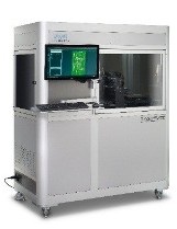 The DragonFly 2020 Pro 3D Printer is a one-stop solution for 3D-printed electronics. It enables electronics makers to move quickly from concept verification and design validation to test fixtures by 3D printing their own professional circuit boards. With the DragonFly 2020 Pro, you can:
- Print high resolution trace and space with the precise inkjet deposition system
- Construct the full range of multilayer PCB features- including interconnections such as buried vias and plated through holes
- Keep sensitive and proprietary design information in-house while developing
- Enjoy the quick production of professional multilayer PCB prototypes, antennas, experimental electronic circuits and more
Product Page Link: http://www.nano-di.com/dragonfly-2020-pro
Contact Details: Galit Beck, Galit@nano-di.com
YAMAHA YSi-V 12M Type HS2 high-end hybrid AOI
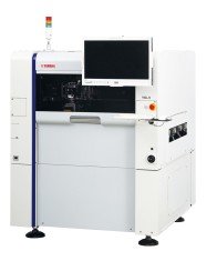 YAMAHA announces the launch of its YSi-V 12M Type HS2 high-end hybrid Automated Optical Inspection (AOI) system. The YSi-V 12M Type HS2 offers faster inspection speed, higher precision, and enhanced capacity and performance for specular components.
Development of the YSi-V 12M Type HS2 targeted faster processing through improved image processing hardware and image inspection algorithms; as a result, it has achieved more than 25% increase in 3D inspection speed when compared to the existing model, and delivers a significant speed increase of up to 40% for Printed Circuit Boards (PCBs) with high component mounting density.
New features include a high-precision mode, enabling capture of clear three-dimensional images. The high-precision 7 μm resolution camera includes an all-new design dedicated 3D image capture projector optical system, significantly improving form reproducibility of extremely small-sized components down to 008004 size, and increasing height measurement repeatability. In addition, the optimization of image capture parameters and the use of newly-developed algorithms has enabled inspection capacity and performance compatible with thin, highly-integrated WLCSP and FOWLP components, whose use has risen dramatically since last year.
The YSi-V 12M Type HS2 is user-friendly and quick to program, but also offers the customer greater flexibility. For example, the user can decrease 3D speeds, allowing the user to either reduce cycle time or increase 3D inspection, resulting increased inspection capability. This allows more flexibility for the customer by allowing more programming options.
Product Page Link: https://global.yamaha-motor.com/news/2017/0601/ysi-v.html
Contact: George Babka, Sales General Manager, george_babka@yamaha-motor.com
Omron’s VT-X750 Automatic X-ray Inspection system
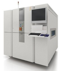 Omron’s VT-X750 Automatic X-ray Inspection system, incorporates the latest solution for manufacturers desiring high quality, in-line, automated X-ray inspection on PCBs, containing components such as BGAs or LGAs and through-hole connectors.
Traditional X-ray technologies are limited in inspecting components like BGAs, LGAs or THT-components. Omron’s VT-X750 incorporates ‘Computed Tomography’ (CT), specifically to provide high-precision, X-ray imaging to perform precise and reliable analysis of these hidden soldered areas. “The VT-X750 can inspect accurately and reliably, soldered defects such as Head in Pillow and voids within BGA and LGA devices”, explains Kevin Youngs, Key Account Manager Europe at Omron Automated Inspection Business Europe. The new inspection system measures also the percentage solder, including voids in QFN’s, and Barrel Fill in through-hole devices.
Traditional AXI systems incorporate 2D or 2.5D X-ray tomography. But these technologies provide limited capability causing high false calls and are insufficient to find core defects such as Head in Pillow and in many cases, voids. The limitation of these systems is the capability to inspect PCB’s with double sided components. 3D-AXI overcomes these deficiencies of traditional 2D or 2.5D system. However, in today’s AXI systems, there are 2 basic forms of 3D X-ray: Tomosynthesis and Computed Tomography.
The VT-X750 inspections are performed very quickly at speeds less than 4 msec. per field-of-view (FOV). Omron strongly believe combining VT-X750 new ultra-fast process times and unique data capturing technology, VT-X750 is the first 3D-CT AXI system that can be utilised into the SMT production Line. “We see this as a great benefit targeted to increase customer manufacturing quality and reduce manufacturing costs”, said Youngs. In comparison to Tomosynthesis, VT-X750 utilises CT reconstruction software and combines multi-slice data with laser displacement technology that gauges the PCB surface for each solder-joint, for example each solder ball of BGA, compensating for any warpage and allowing the system to perform cross-sectional analysis at the proper slice-level locations.
Selectable inspection of 6, 8, 10, 15, 20, 25 or 30 microns combined with selectable numbers out of 512 X-ray projections up to 512, taken from different angles to produce cross sectional tomographic images of specific areas of target area, allow for user-driven variation between higher inspection speeds for production environments, and ultra-high-quality 3D image acquisition for research of defect analysis. “The machine offers benefits for a big group of customers, from automotive suppliers , with high running production lines to midsize companies who need an X-ray also for smaller batches”, so Youngs.
Omron incorporates CT as VT-X750 principle inspection criterion. “The key factor was to develop 3D X-ray technology that addresses the limitations of other 2.5D and other 3D X-ray technologies, thus providing the highest quality solder joint inspection for key industries such as automotive, aerospace, infrastructure, communication and medical”, explains Youngs.
Product Page Link: http://www.ia.omron.com/products/family/3683/
Contact: Omron Europe B.V., aoi.info@eu.omron.com, Website: inspection.omron.eu
Metcal CV-5200 Connection Validation™ Soldering Station
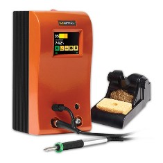 Metcal’s CV-5200 Connection Validation™ Soldering Station provides real-time closed loop feedback on intermetallic compound formation— the world’s first. Plus, a new communication port enables process traceability and firmware upgrades.
Connection Validation™ provides operators with real-time, closed loop feedback, via a green or red light integrated into the hand piece, to indicate intermetallic compound formation—the key to a good solder joint.
It’s the most innovative advancement in soldering technology in almost 30 years and represents a quantum shift in process control—particularly in the prototyping and production of automotive, aerospace, military, medical devices, and other products with zero risk tolerance.
The CV-5200 introduces Connection Validation, groundbreaking technology that evaluates a solder joint’s quality by calculating the intermetallic compound formation and providing closed loop bi-directional feedback to the operator via the LED ringlight located in the hand-piece. The CV-5200 also features:
- 2.8” color LCD touchscreen with easy-to-see graphics
- SmartHeat Power on Demand technology, which senses thermal load and instantly delivers power to the solder joint
- Communications Port for process traceability data and firmware graphics
- Precise tip temperature display
- Integrated Net Power Meter and graph
- Patented Chip-in-Cartridge technology
- Stores and records cartridge attributes
- Provides traceability information
- Protects power supply from non-conforming cartridges
- Backwards compatible with MX series power supplies
- Password protection
Product Page Link: http://info.okinternational.com/metcal-connection-validation
Contact:Dilip Rane, Senior Sales Manager – India and Middle East, OK International. drane@metcal.com
Littelfuse surface mount fuse PICO® 304 Series
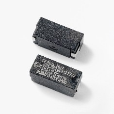 The first encapsulated surface mount fuse designed for intrinsic safety protection of equipment intended for use in or near hazardous locations and explosive atmospheres and certified to the UL 913 Standard. During overcurrent and short circuit fault conditions, the 1mm-thick encapsulation around the body of the PICO® 304 Series surface mount fuse minimizes the amount of heat produced and contains any sparks or arcs inside the fuse assembly, preventing them from being exposed to potentially explosive gases or dust in the environment. This encapsulation eliminates the need to pot or coat printed circuit boards or assemblies, saving production time and money to reduce end-product costs.
The PICO® 304 Series is rated for 277V AC/DC with 1500A breaking capacity, making it suitable for barrier circuits and other circuits separating intrinsically safe circuits from non-intrinsically safe circuits. Available with current ratings from 50mA to 750mA, the series is ideal for limiting fault power available in a circuit, helping to reduce required power ratings and size of downstream components, wiring, and circuit board traces.
Product Page Link: http://www.littelfuse.com/products/fuses/hazardous-area-type-fuses/hazardous-area-type-fuses/304.aspx
Contact:Navneet Vinaik, Field Application Engineering Manager, nvinaik@littelfuse.com, www.littelfuse.com


