CoolMOSTM P6, the latest 600V CoolMOSTM device series, is specifically designed to fulfill power supply applications requirements, addressing at one time the focus on higher efficiency, a nice “ease of use” level, and multipurpose use in the PFC stage and in the DC/DC stage to save design in time and costs.
Nowadays the efficiency requirements for power supplies, especially in light load operation, are getting higher and higher, both in the PFC stage and in the DC/DC stage. To fulfill these requirements, the logical choice for an engineer is to use a MOSFET with a lower Gate charge to reduce the driving losses. The low Gate charge also allows very fast switching for turn on and turn off in the whole load range. However, this choice also has drawbacks. Due to oscillations on the Gate, the engineer has to take a higher RG,ext for slower switching or take a ferrite bead to damp these oscillations.
Either option consumes a lot of engineering time and adds cost to the design. This leaves the engineer with the challenge to identify a power MOSFET which both enables higher efficiency and can simply be plugged-in to a system design without a lot of reengineering time. This second characteristic can be called “ease of use.” Of course, the engineer also must meet this challenge, while also trying to reduce the costs of the Bill of Material. One path to accomplish that is to choose the same MOSFET in the PFC and DC/DC stage; but besides high efficiency and “ease of use” requirements a rugged body diode for hard commutation in the DC/DC stage is needed.
CoolMOSTM P6, the latest 600V CoolMOSTM device series, is specifically designed to fulfill all of these application requirements, addressing at one time the focus on higher efficiency, a nice “ease of use” level, and multipurpose use in the PFC stage and in the DC/DC stage to save design in time and costs.
Target Applications
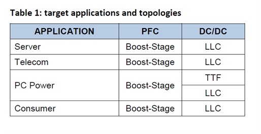
The new CoolMOSTM P6 is designed for different applications of a typical AC/DC SMPS power architecture.
The P6 technology fits in the hard switching PFC stage and furthermore in the soft switching DC/DC conversion stage. This concludes the following target applications for the 600V P6:
The following technical parameters are the key factors for the effectiveness of the P6-technology in this class of applications.
1. Reduced Gate charge (Qg)
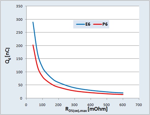
One of the most important improvements of CoolMOSTM P6 is reduction in device gate charge, Qg which brings benefits especially in light load conditions due to reduced driving losses. P6 will offer a 30% Qg reduction in comparison with CoolMOSTM E6 which mainly comes from the reduction of the plateau charge. It also allows very fast switching for turn on and turn off.
2. Integrated Gate Resistor (RG)
To balance fast switching to achieve maximum efficiency while not sacrificing “ease of use” and good controllability the CoolMOS™ P6 comes with a small integrated gate resistor, RG.
This integrated small RG allows fast turn on and turn off at normal operating current conditions but limits di/dt and dv/dt in case of abnormal conditions.
3. High Gate threshold voltage (Vth)
In resonant topologies like LLC and ZVS it is possible to eliminate the turn-on loss but the turn-off loss still represent a big portion in the total loss consideration. A high gate threshold voltage (Vth) enables early turn off of the MOSFET which results in better efficiency.
The earlier CP and E6 technologies from Infineon are defined with the typical Vth at 3V. On this characteristic you can see that the P6-technology will show an increased Vth to typical 4V. Regarding the switching speed, it can be seen that the slope of P6 is much faster than that of E6 and pretty close to CP, which provides low switching losses and gives high power conversion efficiency.
4. dv/dt rating improved to 100V/ns
SJ-MOSFETs have a typical MOSFET dv/dt rating of 50V/ns. Engineers are limited by this datasheet parameter to force fast switching via low RG,ext for high efficiency applications.
Due to the low Qg and the reduced capacitances of the P6, in combination with manufacturing experience gained over 12 years, P6 technology has an improved dv/dt from 50V/ns to 100V/ns.
In Figure 1 the measured dv/dt comparison between E6, P6, and CP in the RDS(on),max range of 190 mΩ is shown. CP has a maximum dv/dt of 50V/ns and a high slope. Compared to CP the P6 technology offers a smooth dv/dt and an improved level of control. Even under a minimum of RG,ext, dv/dt of P6 is still lower than 50V/ns.
The P6 technology is a very robust technology to withstand over 50V/ns without changes in the characteristics. As a result of the improved dv/dt, it is possible to reduce the external RG results to gain efficiency.
“ease of use,” gate ringing of P6
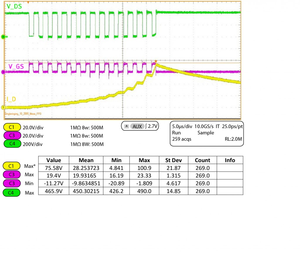
Figure 2 shows a typical switching waveform of IPP60R190P6 in a PFC. This test circuit is configured with an additional external gate to drain capacitance exhibiting 7.2pF for capacitive coupling between gate and drain emulating PCB parasitic capacitance. Designers should put extra care in the layout to minimize this parasitic capacitance to enable the highest performance of the MOSFET. In this measurement, 5Ω external RG for 190mΩ device is used.
Switching waveforms are measured with VDS=400V (shown in green) and VGS=13V (shown in crimson). The current waveform shown in yellow is increasing every pulse up to saturation which is represented with an offset in VDS at the peak current level of 75A. P6 with optimized RG shows a good switching waveform without hurting the VGS specification limit.
Hard commutation on conducting body diode
Hard commutation on a conducting body diode is required for soft switching applications and a tradeoff is required between high commutation ruggedness of the body diode and fast switching. All properties of a fast switching device (high di/dt, low Qg, low RG) result in high voltage peaks during hard commutation on a conducting body diode. Figure 3 shows the voltage peaks under hard commutation followed after 10μs body diode conduction time (in normal operation conditions you will not find longer body diode conduction times than
400ns).
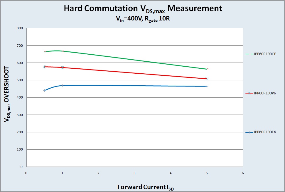
Figure 3 shows the VDSmax overshoot due to high dIrr/dt in a commutation. The device under test is the same as the switch, both with an RG,ext of 10Ω . VDSmax overshoot will be influenced by the parasitic components of the layout, the external RG and the switching speed of the switch. P6 has an improved commutation behavior against CP.
Measurement results
In this section real application measurements will be shown to demonstrate the benefits of
CoolMOS™ P6 in hard- and soft- switching applications.
Efficiency measurement in a 1800W CCM PFC which represents the telecom application
In this measurement the 600V P6 is compared to C6 and CP in the 41mΩ RDS(on) range.
Setup parameters:
• Vin=90VAC
• Vout=400VDC
• Pout=0W to 900W
• Frequency=100kHz
• RG,ext=10Ω, in a plug and play scenario comparing 600V P6, C6 and CP devices
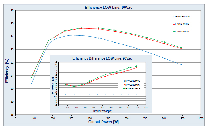
This plug and play measurement shows the benefit of CoolMOS™ P6 in comparison to CoolMOS™ C6 and CoolMOS™ CP. At 10% light load condition P6 has an efficiency improvement over 0,45% and in full-load, 1,25% compared to C6. This efficiency benefit results due to Qg reduction and relatively high Vth.
Efficiency measurement in a 200WPC Silverbox in LLC stage
In this measurement the 600V P6 is compared to E6 and CP in the 280mΩ RDS(on) range.
Setup parameters:
• PC Silverbox LLC stage 200W
• Vin=90VAC
• Vout=400VDC
• Pout=0Wto 200W
• Frequency=65kHz
• RG,ext, turn,on=27Ω
• RG,ext, turn,off=10Ω
• Plug and play scenario comparing 600V P6, E6, and CP
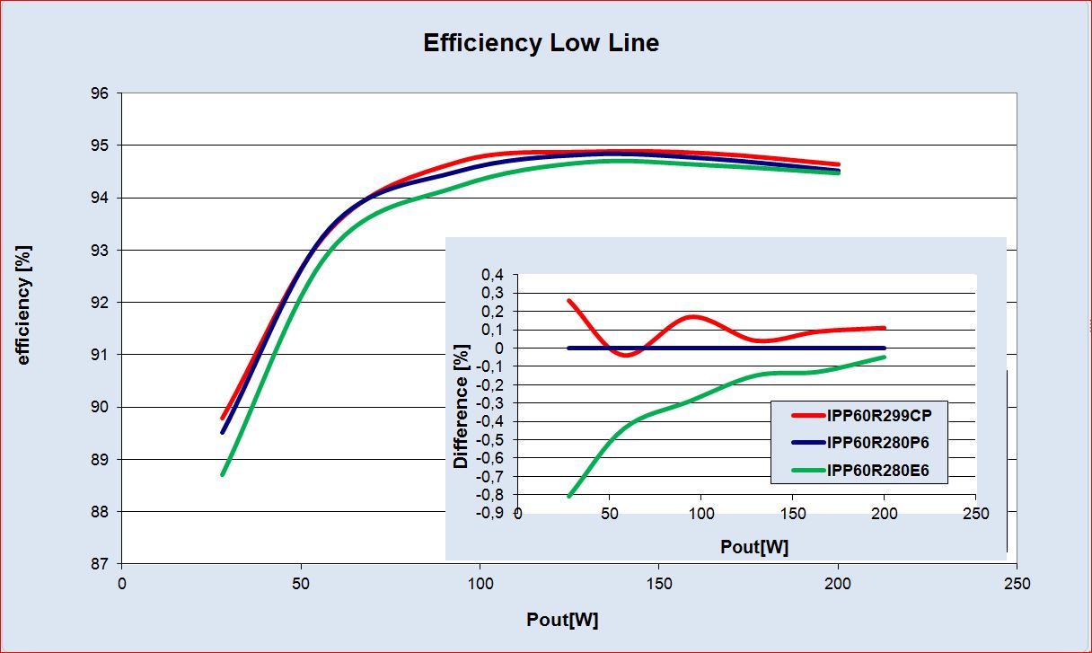
In this LLC measurement, P6 shows an efficiency benefit against E6 over 0.8% in light load.
This improvement is also based on Qg reduction of 30% compared with E6. At the full load,
P6 and E6 give similar efficiency measured results due to the same RDS(on) level which is the important parameter at full load.
Design Guideline for using 600V P6
In the following sections some guidelines are given how to use the CoolMOSTM P6 in the best way to enable an optimized performance.
Minimum external gate resistor (Rg,ext)
In well designed power supply we recommend to use a very low ohmic external resistor in the range of minimum 5ohm for turn on and zero ohm for turn off. This efficiency driven Rg selection could be taken due to an implementation of an Rg,int and the very robust design of
CoolMOSTM P6. However, the selection on external Rg is always a function on the PCB parasitic components which generates an unexpected voltage- or current- peak on the MOSFET due to voltage signal from L stray *di/dt and current signal from C parasitics *du/dt. To prevent such peaks a reduction of the parasitic components or an increased Rg,ext for the MOSFET is recommended.
Paralleling of 600V P6
For paralleling 600V P6 we generally recommend the use of ferrite beads on the gate or separated totem poles driving circuit.
Conclusion
In today`s MOSFET market, a huge number of devices offer different behavior in ease of use and achievable efficiency. Several devices offer easiest controllability resulting in best ease of use with only some degree of efficiency tradeoff. Some devices offer the highest efficiency but due to the aggressiveness in switching these, they require extra care in the design. The introduction of CoolMOSTM P6 surmounts this problem: with this device the demand for high efficiency is being met without sacrificing the ease of use. This was made possible through a well-balanced technology offering optimum ease of use and performance of the device.
Additional Information
The Infineon page www.infineon.com/p6 provides access to detailed information regarding the 600V CoolMOSTM P6, e.g. Power Management Selection Guide 2013, Application Note 600V CoolMOS™ P6.
Author Profile

Alois Steiner was born in Villach/Austria and studied microelectronics.
For six years he has been working as an application engineer for High Voltage at Infineon Technologies AG. He focuses on customer requirements and their application needs.
Alois Steiner released several application notes and technical articles on CoolMOS™ families like C6, CFD and P6.


