Innovation breakthrough in circuit carriers
MULTIPLE DIMENSIONS AG, with its 3D-MID (Molded Interconnect Devices) technology, supports the modularization and miniaturization in industrial electronics. Product developers will be open in the use of the third dimension and have the highest degree of freedom in creating forms.
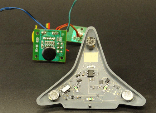 The applications of injection molded interconnect devices are enjoying a rapid increase in customer base – and an innovation is only truly realized once it succeeds in penetrating the market.
3D-MID technology is the latest refinement and most recent high point in the history of the circuit carrier. It extends the range over conventional rigid and flexible printed circuit boards. The highlights of the PCB started in 1925 with the first patent and prototypes by Charles Ducas and later by M. César Pasolini; in the 50s the first printed circuit boards were one-sided and double-sided construction with assembly; first in the 60s was the patent for multi-layer printed circuit boards; 1982 saw the introduction of SMT (Surface Mount Technology); and the 90s witnessed further developments regarding flexible and rigid-flexible printed circuit boards. The global production value of the printed circuit board industry was in 2014 USD $59.6 billion with an increase of 3.7% compared to the previous year-2013.
Benefits
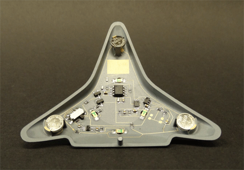
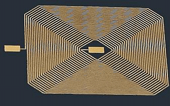
The advantages of injection-molded interconnect devices (3D-MIDs) are manifold. In particular, the three-dimensional design space to connect technology modules, components, etc. is optimized via rounded edges. The antenna designs are virtually unlimited. Antennas based on the 3D-MID Technology have found worldwide distribution in mobile phones. Shields can be easily realized. The placement of LEDs and other SMT components allow spatial orientation effects which are difficult to implement on the two-dimensional PCB structure. The high-quality marking of characters or symbols is yet another possible application.
Process Steps
The five process steps for injection molded interconnect devices: (1) manufacturing injection mold, 2) injection molded plastic, 3) laser structuring, 4) chemical plating, and 5) SMT assembly) contribute to the efficiency and cost savings for the production of desired components or modules. In particular, in many applications on printed circuit boards the connecting cables can be eliminated. In an overall cost analysis the reduction of cost results from saving on assembly costs such as wire connections, soldering, assembling, screws, etc. combined with saving materials such as wires, screws, adapter plug, mounts, etc. The functionality of an application is optimized and massively simplified. These savings help to compensate for a more expensive thermoplastic material, which is doped with laser-activated metal compound additives. The laser beam decomposes the plastic matrix in a volatile excitation on the surface and exposes the additive metal nuclei, which are very fine and rest within in the microstructures of the roughened surface. A slight erosion of the plastic to the laser-machined surfaces takes place. The now exposed metal particles act as nuclei for the subsequent metallization step. In the following electroless baths copper, nickel and gold the interconnect layers are formed on the lasered part surfaces.
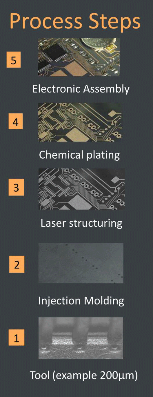
The five process steps for laser-structured circuit carrier.
Plastic meets electronics!
The widespread use of 3D-MID antennas in the mobile phones have already been mentioned. Various applications in the automotive industry, and in industries such as watches, medical technology, consumer and industrial goods to name a few, confirm the penetration.
Applications
Multiple Dimensions AG
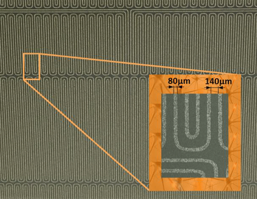
Multiple Dimensions AG was founded by four successful entrepreneurs who bring a history of proven innovations and decades of industry experience, reaching every continent where innovative products are used. Multiple Dimensions AG is a powerful and creative producer and developer of 3D-MID applications. The responsibility of Multiple Dimensions is to provide the 3D-MID technology and reveal its advantages for clients and end users, to unlock new dimensions in miniaturization, cost savings and spatial optimization. The name “Multiple Dimensions” reflects opening up new dimensions of weight savings, positioning of components and design options like labeling or other aesthetic choices; and capability for space/trace conductors of 80um/80um further enables the dimension of miniaturization.
Headquartered in Bruegg, Switzerland, Multiple Dimensions and its partners maintain operations across the globe. A modern factory, a worldwide technology and distribution network has been established. Multiple Dimensions AG has a current customer base of well-known global companies in the segments of industrial, medical, automotive, instrumentation and communications.


