Multiple Dimensions shows new approaches to MEMS and sensor devices
The trend towards miniaturization is affecting more and more sectors. Contributing to the simplification of electronic systems, 3D-MID (Molded Interconnect Device) technology offers compelling solutions. Current market penetration is found in applications for automotive, medical, electronics and watchmaking industries. What are the advantages for the MEMS industry?
Technological leadership and competitive advantage with MIDs
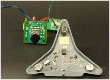
Today, 3D-MID components serve in a range of established applications including sensors in the automotive industry, connectors for medical equipment, and millions of antennas produced annually for smartphones. New innovations are not limited to any particular sector and include unique switches, novel Microelectromechanical Systems (MEMS) and LED applications. These applications advance the miniaturization trend while also simplifying assembly and saving on system cost. MID technology is recognized by developers for increasing design freedom by eliminating the confinement of traditional 2-Dimensional PCB layouts and allowing for more electronic features in smaller volumes.
MEMS – Application
3D-MID technology is established in several connectivity solutions and coming into increasing use for MEMS integration. 3D-MID allows for integrating both mechanical and electronic functions into one part with a construction that is much more compact while also achieving much greater function density. More and more applications involving electrical and electro-optical circuits are made using 3D-MID technology.
3D packaging, Package on Package (PoP) or System in Package (SiP) are key technologies to realize high functional integration into the smallest space. However, while PoP or SiP deal with packaging on chip level, the chip itself has to be assembled to a substrate. The substrate in turn has to be connected electrically and mechanically to its functional environment. The solution for the 3D assembly and 3D connectivity is offered by the 3D-MID technology.
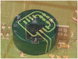
The possibility to integrate mechanical and electrical functions in one module shows real strength in electronic assembly applications like MEMS packaging and sensors packaging.
BGA-Packaging – Application
The miniaturization abilities of 3D-MID are also applied to packaging of microprocessors such as traditional BGA (Ball Grid Array). The advantages of BGAs include a small footprint and good heat dissipation to the PCB. But BGAs have some disadvantages. One of the main problems is their sensitivity to mechanical and thermal stress. The ball may not endure the stress of vibration or heating of electronic equipment and this leads to failure.Multiple Dimensions developed a processor housing that eliminates the disadvantages of the BGAs. This solution involves the BGA substrate being replaced with a selectively metallized molded part, produced by the 3D-MID technology. The plastic component constitutes the carrier for the chip and the contacts.
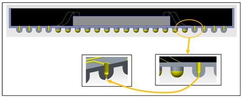
Benefits of this solution
- Stable mechanical connection consisting of one part
- Reliable contacting since structures and contacts are one – no interface.
- Fewer parts, no extra balls or pins, the substrate can also serve as housing
- Less height because of fewer components
- Improved thermal management with integration of heat sinks made with additional metallized surfaces on the substrate and/or and over-molded heat sink insert
- Lateral connection of processors to other electronic components is possible with the substrate housing structured and metallized with additional traces and pads.
- Economy (fewer components, fewer process steps, fewer sources of error)
Market trends: Internet of Things (IoT) & Industry 4.0
The rapid expansion of the Internet of Things (IoT) will increase demand for MEMS devices. According to the research institute IHS the worldwide sales of USD $16 million increase in 2013 to $120 million in 2018. The applications can be found in a variety of industries, from tracking systems, Hearables (audio) and wearables, to building automation and the smart grid.
Industry 4.0 describes the fourth industrial revolution in the industry. The networking of people, machines and the shop floor will transform production sites into smart factories. For this to happen sensors are required to provide real-time information on material status, temperatures, locations, etc. Such sensors will be integrated within all active objects making up the productive workplace. By integrating antenna structures directly on the MID-MEMS, the data can be relayed directly from the sensor – with no additional costly RF components.
MID-Production – Plastic meets electronics!
There are two main approaches to manufacturing 3D-MID products. The process of laser direct structuring (LDS) is widespread and is now established around the globe. With LDS, a single physical form is created with plastic injection molding. Thanks to the 3D design freedom of modern molding, the shape is nearly boundless. The molded thermoplastic contains a non-conducting organic-metal complex as an additive. As the laser scribes the desired circuit layout over the surface of the component, metal nuclei within the additive are activated, becoming attractive sites for metal plating. Chemical plating then applies copper, nickel and gold layers to transform the plastic part into a three-dimensional circuit carrier. Multiple Dimensions AG is dominant in the LDS process but also produces 3D MID products using 2K, also known as the “2-shot” process. With 2K two different plastic materials are injection –molded side by side, with one material attractive to chemical plating the other material is more inert and acts as the electrical insulator.
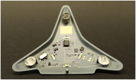
Applications
