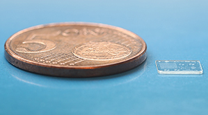
The technology replaces the curved camera lens with very tiny sensor that uses a spiral shape to map light and relies on a computer to figure out what the resulting image should look like. This is the beginning and the stepping stone for new technologies with an idea of smaller and simpler.
By Rachel Metz : Patrick Gill is excited to show me a small, fuzzy-looking picture of the Mona Lisa, printed in black and white on a piece of paper. It’s not much to look at, literally, but it’s unmistakably her, with long dark hair and that mysterious smile.

More intriguing than the low-resolution image of da Vinci’s masterpiece, though, is how the picture was created: with a lens-free camera that, at 200 micrometers across, is smaller than a pencil point.
While digital cameras with lenses can take great photos, it is difficult to get cameras into smaller devices. Miniaturizing lenses only works to a certain point: the smaller they get, the more difficult it is to make their precise curved surfaces. Gill, a senior research scientist at the technology licensing companyRambus, thinks one way to solve this problem is by replacing the curved camera lens with an itty-bitty sensor that uses a spiral shape to map light and relies on a computer to figure out what the resulting image should look like.
Eventually, he envisions the tiny camera being built into all kinds of things, from wearable gadgets to security systems to toys, without having to add to the cost or bulk of a camera with a lens. “Our aim is to add eyes to any digital device, no matter how small,” he says.
The point is not to build high-resolution cameras like you’d want on a smartphone but rather to build the smallest, cheapest, easiest-to-make optical sensor that can still capture enough information to show what’s going on.

Gordon Wetzstein, a research scientist at MIT Media Lab’s Camera Culture Group, is optimistic about the technology, though he says it’s still not clear how well it will work. “Other than pixels getting smaller, we haven’t really seen much progress in camera sensors for a while,” he says.
Gill shows me a prototype sensor at Rambus’s Sunnyvale office that has been etched with 28 different types of diffractive structures—spirals and other shapes like a cross and a pentagon. A tiny segment of the chip contains a spiral that has been used to capture a number of images, including the Mona Lisa picture Gill shows me as well as fuzzy depictions of John Lennon and Georges Seurat’s Bathers at Asnières.
When you take a picture of a painting on a wall with a regular digital camera, a lens focuses each point of light it captures on a sensor, generating a digital file that a computer can show you as an image. Rambus’s approach instead uses a grating etched with a spiral pattern through which light can enter from every orientation. The sensor below the grating captures a jumble of spirals that a human wouldn’t see as a recognizable image, but software can translate into one.
Gill uses the Mona Lisa image to demonstrate. He shows me a regular black-and-white image of the painting, a blurred black-and-white form indicating the jumble of spirals the sensor would capture for the computer to interpret, and a blurry but still recognizable black-and-white image of the painting as reconstructed from this data by software.
Gill says Rambus’s algorithms let users ask the computer to produce images at various resolutions; the highest he’s done thus far with prototypes is 128 by 128 pixels, which he says represents the capabilities of the highest-resolution sensors Rambus would make if it commercializes the technology.
While there are other lensless camera projects out there, such as one created by Bell Labs (see “Bell Labs Invents Lensless Camera”), Gill believes the one Rambus is working on is less complex and can be made much smaller. The technology used to make it is similar to the CMOS technology used to construct computer chips, so it could be manufactured within an array of chips while adding just a few cents to the overall cost of each chip.


