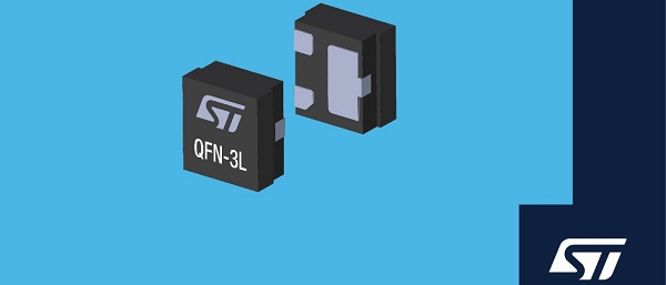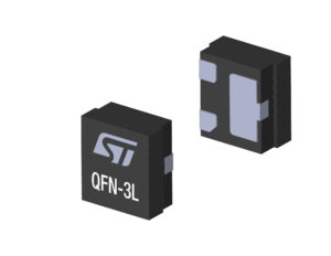
ST is launching today the ESDCAN03-2BM3Y, the first automotive-grade transient voltage suppressor for CAN buses with a line capacitance of only 3.3 pF and a clamping voltage of 33 V at 1 A in a small DFN1110 package. The device comes as a direct result of the mind-blowing challenges engineers face when designing control units for cars. With the increase of sensors and processing units, designers must pack a tremendous number of components on a small surface. Moreover, some of these components are critical for the safety of the driver and passengers. For instance, collision avoidance systems, airbags, or antilock breaking all use a Controller Area Network bus (or CAN bus). Problems arise when integrating many CAN controllers on a PCB the size of a notepad. Besides space constraints, a packed system suffers from numerous electrical issues engineers must overcome before they can ship their design.
The Benefits of a Comprehensive Strategy
Design teams contend with a vast number of manufacturers and solutions, which can get dizzying. The ESDCAN03-2BM3Y is thus unique not only because of its electrical capabilities but because it represents another building block in ST’s overall automotive strategy. When engineers look for a microcontroller, they can turn to the SPC5 MCUs. Need a more precise GNSS receiver? The TeseoV is the only dual- and triple-band model today. From rear lighting systems to power management and more, teams benefit from better support and more cost-effective solutions when they work on more aspects of their project with the same partner. The new TVS device is another reminder of our desire to offer complementary solutions in the automotive space. With the ESDCAN03-2BM3Y, we provide a new way to protect CAN buses from density and reliability challenges.
ESDCAN03-2BM3Y: A Solution for High-Density PCBs
The Space Challenge

The most apparent challenge when dealing with a highly dense PCB is its space constraint. However, designing a TVS in a smaller package is in itself a complex problem to solve. In previous generations of devices, ST sometimes integrated more than one die under one roof. Moving to a smaller housing necessarily limits the number of dies that we can use at once, which negatively affects performance. Hence, our engineers needed to find a solution to improve performance while using only one die and a smaller package.
The innovation that made the ESDCAN03-2BM3Y possible came from what ST calls “Vertical Technology”. Originally used in components for smartphones, it employs a vertical PN junction. As a result, the signal enters by the top of the device and leaves by the substrate’s bottom and vice-versa. ST can now use this technology in the ESDCAN03-2BM3Y because our teams managed to adapt it to a 24 V device. Beyond enabling a smaller package, using a vertical structure means that electrical paths are significantly shorter. As we move from millimeters in horizontal technologies to micrometers, our solution enjoys a much lower resistive path, positively impacting the overall performance.
The Parasitic Challenge
Another issue that engineers working on high-density PCBs must overcome pertains to parasitic interferences. Indeed, there are so many tracks on the board that designers know they will have to deal with inductance issues. Hence, devices that protect CAN buses must have an inherently low capacitance to avoid compounding the problem. The challenge is so critical that car manufacturers themselves came up with hard limits, most of them demanding that devices protecting CAN buses have a line capacitance of less than 6 pF. However, obtaining a low capacitance is challenging because the tradeoff can negatively impact the component’s other electrical properties.
The ESDCAN03-2BM3Y is, therefore, unique in the industry because it achieves a line capacitance of only 3.3 pF, far below manufacturers’ requirements, which then gives engineers more headroom when dealing with other components. ST managed such a feat thanks to its new packaging technology and the device’s architecture. Our R&D engineers adapted the latest die technology structures used in smartphones to minimize parasitic capacitances from active areas. As a result, we significantly lower the overall line capacitance. Put simply, our engineers optimized the architecture to offer far better specifications than any other competing device today.
The Transient Coupling Challenge
Finally, a third difficulty that may arise within a packed PCB comes from transient couplings. The presence of numerous components on a tiny surface means that the transient voltage suppressor must be as close to the CAN connector as possible to avoid propagation of an electrostatic discharge that could damage nearby devices. It’s the reason why engineers closely look at their TVS’ clamping capabilities to see how much voltage passes through when facing a surge. The problem for many engineers is that a lower line capacitance tends to increase the clamping voltage. And, as we previously saw, car manufacturers demand a low line capacitance.
The ESDCAN03-2BM3Y solves this conundrum by offering the lowest line capacity and lowest maximum clamping voltage, compared to competing devices. ST engineers achieved a clamping voltage of 32 V at 3 A thanks to the device’s low dynamic resistance. Indeed, improving the package makes it possible to optimize the die size, thus offering better clamping performances. Comparatively, most competing devices have a clamping voltage of more than 40 V at 1 A. Importantly, companies often pay close attention to these numbers as they are synonymous with a more robust implementation.
ESDCAN03-2BM3Y: A Solution for Next-Generation Cars
The Manufacturing Challenge
After engineers evaluate the specifications of a device, they often move onto the qualification stage, which can get tricky. Even if teams find the best TVS ever made, models incompatible with large-scale productions are unusable. Additionally, manufacturers will often establish a mission profile, a document that sets minimum reliability requirements. For instance, a company will demand that a TVS run for a minimum number of hours at a particular temperature. The problem comes when the company behind a transient voltage suppressor doesn’t run tests that match the mission profile. In this instance, the TVS maker would have to run new trials, which are time-consuming and may delay a particular project.
Wettable Flanks
The ESDCAN03-2BM3Y is mindful of those issues and offers solutions in the form of wettable flanks and a certified junction temperature of 175 ºC. The former is an inherent feature of the DFN1110 package. With traditional bottom pads, the only way to evaluate a solder joint is to use an X-ray image. The problem is that the process is expensive and cumbersome, thus contributing to increased manufacturing costs. Wettable flanks solve this by moving the solder joints to the side, thus enabling an automated visual inspection. As a result, engineers can expect to significantly lower costs of ownership and manufacturing.
High Junction Temperature
The ESDCAN03-2BM3Y also stands out in reliability measurements as ST certified a junction temperature of 175 ºC. The number itself may sound boastful since nothing in the car will reach this number. However, the reason we continue to offer such a rating is to ensure that we meet every single mission profile currently enforced. Engineers won’t have to ask ST to run more reliability tests, and they won’t have surprises. We already ran benchmarks at temperatures that exceed what the industry is looking for. As a result, companies will rapidly know if the component will meet their requirements.
The EV Challenge
Design teams are facing a new challenge with the electrification of vehicles in the form of leakage currents. Manufacturers always had strict requirements but now more so than ever. Indeed, engineers must deal with the fact that an electric car parked and not charging must still start even after several weeks of downtime. Hence, since leakage currents drain the battery when the car is in sleep mode, it is crucial to keep them to a minimum, or users won’t trust their vehicle to work reliably. As a result, many car manufacturers required their TVS to have a maximum leakage current of only 100 nA. The EDSCAN03-2BM3Y far exceeds these expectations with a leakage current of 50 nA. As a result, engineers get more headroom, which will simplify their design operations.
Click Link- https://blog.st.com/esdcan03-2bm3y/


