By Barry Manz, Mouser Electronics
Not only is the performance of FPGAs and other logic devices becoming more formidable, these devices are incorporating functions typically performed by other types of logic, CPUs, GPUs, and DSPs. They’re the semiconductor versions of the Swiss Army Knife.
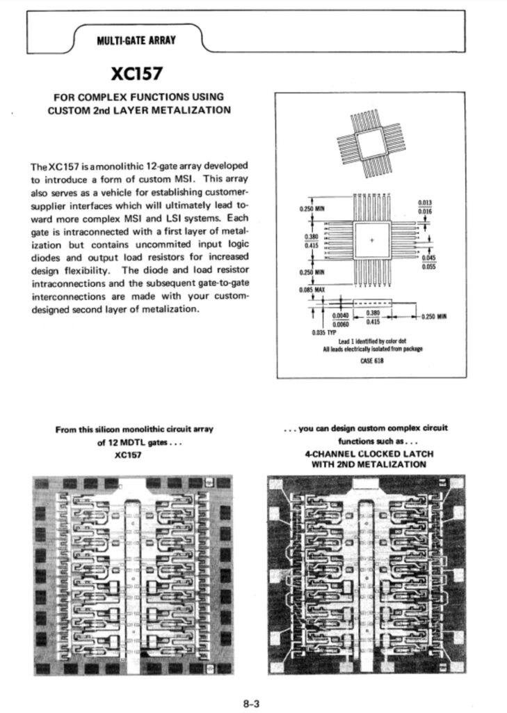
In 1969, when hundreds of thousands (including the author) partied at Woodstock, the Concorde made its first trial run, and Richard Nixon was inaugurated, another momentous event occurred: The XC157 mask-programmed gate array with 12 gates and 30 input/output pins appeared in the 1968 edition of the venerable Motorola Semiconductor Data Book (Figure 1). It may not have shaken the world, but for the electronics industry it was like planting a flag on the moon, as it (and efforts by many others at the time) marked the time when programmable logic devices became a commercial reality.
To use a time-worn phrase, the rest is history – and what a history is has been, with dozens of different logic types created by many companies arguably making all types of embedded systems possible.
The various logic types can be grouped into three categories based on their comparative level of complexity (Table 1). The top of the hierarchy is the domain of field-programmable devices–FPGAs and their variants– that have come a very long way since David W. Page and LuVerne Peterson in 1985 initiated the concept. The differences between FPGAs and their nearest brethren, Complex Programmable Logic Devices (CPLDs), are their ability to perform more complex functions and that they are a “blank canvas” on which their functions must be painted rather than being previously endowed by the manufacturer with specific functions.
 This makes FPGAs extraordinarily versatile, as they can perform computing, signal processing, high-speed communication, and other functions without external peripherals. Defining the vast number of connections and cell logic functions in an FPGA was never easy and of necessity, FPGA manufacturers and design software vendors have developed software tools that make the process less onerous. Predesigned and verified intellectual property (IP) functional blocks are also available to help speed the programming process.
The initial FPGA concept was followed in the late 1980s by the results of a U.S. Naval Surface Warfare Department program in which industry participants developed a computer that implemented 600,000 reprogrammable gates. Shortly thereafter, the first commercial FPGA was (the XC2064) was unveiled by Ross Freeman and Bernard Vonderschmitt in 1985 who founded Xilinx. It was an 8 x 8 configurable logic block (CLB) grid (64 CLBs) with two three-input look-up tables (LUTs).
Fast forward to today, and it shows as to how startling progress has been. FPGAs now integrate ARM Cortex or other processor cores, can perform more than 1 trillion floating-point operations per second (teraflops) for DSP, integrate ADCs, have total throughout (all serial transceiver channels) of nearly 3 Tb/s, up to 50 million logic elements, very-high-speed memory (and lots of it), and 128-b encryption. All this and more is contained in a single device that has very low power consumption, less latency than ever, and other impressive attributes. FPGAs can now perform so many different type of functions that they are not only a system on a chip, but an extremely flexible and complex one, as well. For example, while communication systems once employed a bank of ASICs to implement their receiver front-end functions, today they can all be handled by a single FPGA. Unlike an ASIC whose functions are fixed during fabrication, FPGAs can be reprogrammed, generally without hardware changes.
The Next Frontier for FPGAs
The next major step for FPGAs may be their use in reconfigurable computing, where along with software they provide all of the functionality of a computer, with a general-purpose processor used only for control. It’s not a new concept, having first been described in the 1960s and first demonstrated in 1991 by Tom Kean, Dr. John Gray, and Dr. David Rees of Algotronix with their CHS2X4. It was based on the company’s CAL1024 FPGA, which had 1024 programmable cells in 1.5-µm double metal CMOS, and was the first FPGA to provide random access to its control memory and to provide input/output signal sharing to enable arrays of devices to be constructed. The achievement and the technology that enabled it was so impressive that Xilinx acquired the company in 1993.
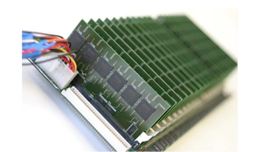
Using FPGAs for reconfigurable computing has been used in some specialized high-performance systems, including cryptography. An interesting example of such a code-breaking machine is Cost-Optimized Parallel COde Breaker (COPACOBANA), which is optimized for running crypt analytical algorithms like the Data Encryption Standard (DES), as well as for other parallel computing problems. It’s not general-purpose in any sense, as its communicaitons are limited in speed and bandwidth and clock rates are much lower than a CPU-based computer. However, it’s also much less expensive and is very powerful in the applications for which it is best suited. By using only FPGAs and other off-the-shelf parts, it’s a fraction of the cost of a CPU-based cryto-computer like the Electronic Frontier Foundation’s DeepCrack.
COPACOBANA (Figure 2) uses 120 FPGAs (plus or minus depending on its specific design) and fits into three units of a 19-inch rack. It devours 48 billion DES decryptions per second while consuming only 600 W, and for control needs only a garden-variety PC running Windows or Linux. In the Cryptographic Hardware and Embedded Systems 2006 (CHES 2006) Workshop’s secret key challenge, COPACABANA took 21 hr., 26 min, 29 s using 108 of its 128 processors at a throughput of 43.1852 billion keys per second. It found the key after searching through 4.7% of the key space. Hardware of this type is used in custom hardware attacks to unlock encrypted transmissions by literally guessing the key or password.
The Wide World of FPGAs
“Logic” would dictate that the versatility of FPGAs would result in a wide range of models, each with specific and sometimes unique attributes designed to meet the needs of different applications. Some of the most demanding of these are defense radar, electronic warfare, and signals intelligence, whose demands are so severe that it’s difficult to believe that any system short of a supercomputer could possibly satisfy them. Yet FPGAs have taken the defense industry by storm, thanks to their massively-parallel processing power and I/O, comparatively low power consumption, and most recently their ability to harness the power of floating-point arithmetic, which is the key to solving many types of computing problems.
Serving these applications are powerhouse FPGAs like Altera’s Stratix 10 family with more than four million logic elements that are manufactured in the Intel 14 nm Tri-Gate process, and incorporate 64-b quad-core ARM Cortex-A53 processors. Compared to their predecessors, they have four times the processor data throughput, four times the serial transceiver bandwidth, a 28-Gb/s backplane, 56-Gb/s chip-to-chip/module speed, more than 2.5 Tb/s bandwidth for serial memory, and more than 1.3 Tb/s bandwidth for parallel memory interfaces with support for DDR4 memory at 3200 Mb/s. To handle the aforementioned need for floating-point operations, they offer more than 10 TFLOPs of single-precision DSP performance.
Overall, they consume 70% less power than previous generation high-end FPGAs with single-precision floating point efficiency 100 GFLOPS/W. The Stratix 10 devices are supported by Altera’s advanced development and debug tools like Altera SDK for OpenCL, SoC Embedded Design Suite.
In the mid-range are Altera’s instant-on MAX 10 FPGAs (Figure 3) integrate DSP, analog blocks with 12-b ADCs and a temperature sensor, PLLs and low-skew global clocks, embedded soft processor support, memory controllers, up to 736 Kbytes of dual configuration flash allowing you to store and dynamically switch between two images on a single chip. They’re built on TSMC’s 55-nm embedded flash technology enabling instant-on configuration so they can control power-up or initialization of other components in the system. Densities range from 2,000 to 50,000 logic elements. Other features include up to 500 user I/O pins, 18 analog input channels, and 128-b AES encryption.
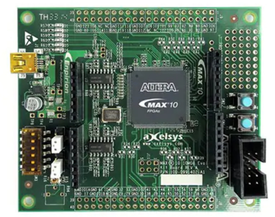
Of particular interest is Nios II that combines a Nios II processor core, on-chip peripherals and memory with interfaces to off-chip memory. The Nios II processor is a configurable “soft” IP core as opposed to a fixed microcontroller, which means the processor core is programmable and not fixed in silicon. As it is implemented on the FPGA, it allows software and hardware engineers to work together to optimize the hardware and test the software running on it.
Even FPGAs that serve most mainstream applications have daunting performance. For example, Lattice Semiconductor says that its MachXO3 FPGA family is the smallest, lowest-cost-per I/O platform targeted at expanding system capabilities and bridging emerging connectivity interfaces using both parallel and serial I/O such as MIPI, PCIe, and Gigabit Ethernet. Their package technology eliminates bond wires, which reduces cost and increases I/O density. Depending on the model they have from 640 to 6900 look-up tables. Typical applications include consumer electronics, computing and storage, wireless communication, industrial control, and automotive. Their design tool library include popular logic synthesis software, pre-engineered IP, and free reference designs optimized for the MachXO3L family.
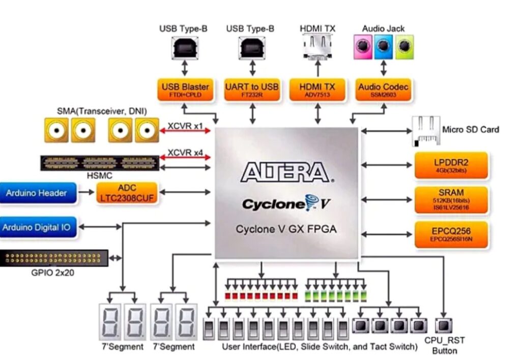
To make things easier, Terasic, which produces optimized subsystems using FPGAs (and other devices), offers the Cyclone V GX Starter Kit hardware design platform built around Altera’s Cyclone V GX FPGA. The board (Figure 4) includes hardware such as an Arduino Header, on-board USB Blaster, and audio and video capabilities along with high-speed transceivers. The company’s goal is to simplify the task of evaluating and prototyping subsystems based on the FPGA with the addition of only a Windows-based PC.
Not the Only Player on the Board
FPGAs may be sexy (in engineer parlance) but they are not the only programmable logic devices out there; other devices can provide a broad array of functions within a single device. Consider the “programmable system on a chip” (PSoC) architecture from Cypress Semiconductor, which is the industry’s only programmable embedded SoC that combines a high-performance analog block, PLD-based programmable logic, memory, and a microcontroller on a single chip that is notable for its frugality with power. The most advanced PSoC variant, the PSoC-5 family, integrates the latest ARM Cortex-M mixed-signal solutions.
The CY8C56LP member of the PSoC-5 family for example (Figure 5) provides configurable blocks of analog, digital, and interconnect circuitry configured around a CPU subsystem. The combination of a CPU with an analog subsystem, digital subsystem, routing, and I/O makes it very appealing for a broad swath of consumer, industrial, and medical applications. The PSoC’s digital subsystem effectively connects a digital signal from any peripheral to any pin through its digital system interconnect, while functional flexibility is afforded via an array of small, fast, low-power universal data blocks (UDBs).
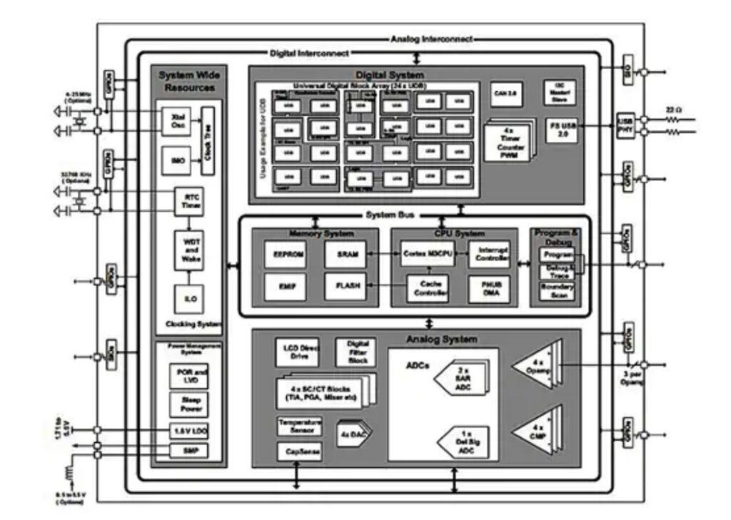
It is supported by the PSoC Creator library of tested, standard digital peripherals (UART, SPI, LIN, PRS, CRC, timer, counter, PWM, AND, OR, etc.) that are mapped to the UDB array. Each UDB contains programmable logic functionality and a small state machine engine that allows it to support a wide variety of peripherals. Other configurable digital blocks can be used for specific functions such as four 16-bit timer, counter, and PWM blocks, I2C slave, master, and multi-master, as well as USB and CAN 2.0. This very device is usually marketed as an MCU, but shares much of the flexibility that an FPGA would have, and is fairly easy to program.
Summary
If by this point the powerful and versatile nature of today’s programmable logic devices is not apparent, consider this: It is possible today to construct a complete signal capture and processing subsystem using only three cards in the OpenVPX form factor (for defense systems.) The major devices include two high-end FPGAs, top-drawer ADCs and DACs (two each), an Intel Core i7 quad-core processor, SERDES transceivers, memory, and I/O. Thanks to the broad bandwidth and high sampling rate of the DACs and the intensive processing power of the FPGAs, this three-card solution can even directly capture signals off the air from DC to 6 GHz. Accomplishing this only a few years ago in such form factors would have required a solution 5 to 10 times the size.
Achievements like this are occurring with increasing rapidity as more market sectors, from consumer electronics, to image processing, automotive and defense electronics, industrial automation and control, and medicine, are taking advantage of what these devices can do. So while FPGAs and other programmable logic devices as a category are not new, they are accomplishing feats that certainly are on the cutting edge.


