
Scientists at Dongguk University have found a way to create printed p-channel thin-film transistors by using the abundantly available and environmentally-friendly copper(I) iodide semiconductor at room temperature. Their energy-efficient and cost-effective fabrication method for these transistors may pave the way for developing low-cost and novel optoelectronic devices.
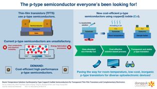 Transistors are the building blocks of most of the electronic devices we use every day, and research on fabricating new types of semiconducting materials for thin-film transistors (TFIs) has been ongoing for decades. Whenever new transistors or novel fabrication methods are discovered, many previously impossible applications become feasible, such as ultrahigh-definition transparent displays and flexible electronic devices. Nowadays, there is a huge demand for p-type transparent semiconductors (which are conductive due to the movement of charge carriers called “holes”) for making p-channel transistors, but when compared to the n-type counterparts, their use is limited by chemical instability and poor electric properties.
To overcome these limitations, a research team at Dongguk University led by Prof. Yong-Young Noh focused on developing a p-type transparent semiconductor for TFTs using a metal halide-like copper(I) iodide (CuI), instead of metal oxide. “The naturally abundant and environmentally-friendly constitutional elements of CuI make it more appropriate for large-scale printed transparent electronics. More importantly, CuI has a higher hole mobility than other p-type oxide-based semiconductors,” explains Prof. Noh.
However, CuI had been barely used as a semiconductor for TFTs because its hole concentration is so high that it results in uncontrollable conductivity (transistors are generally meant to be easily turned on and off at high speeds, that is, they are meant to be switchable from a conductive to a non-conductive state). Moreover, standard solution-based processing for making thin films generally requires a heat treatment called “annealing,” which is energy and time consuming.
The researchers found out that it is possible to reduce the conductivity of CuI-based thin films by making them even thinner and thus suitable for fabricating TFTs with the performance that is currently in demand for many applications. Additionally, these CuI thin films do not require annealing at all and can be processed at room temperature. This saves energy and makes them more cost-effective.
The team tested multiple processing conditions and fabricated various different TFTs to determine the origin of the enhanced device properties and to demonstrate the potential uses of CuI as a thin-film p-type semiconductor. “We believe that this work opens the floodgate for room-temperature, low-cost, printed transparent p-type transistors for diverse optoelectronic devices,” concludes Prof. Noh.
Reference
| Authors: | Ao Liu1, Huihui Zhu1, Won-Tae Park1, Seok-Ju Kang1, Yong Xu*1, Myung-Gil Kim*2, and Yong-Young Noh*1 |
| Title of original paper: | Room-Temperature Solution-Synthesized p-Type Copper(I) Iodide Semiconductors for Transparent Thin-Film Transistors and Complementary Electronics |
| Journal: | Advanced Materials |
| DOI: | 10.1002/adma.201802379 |
| Affiliations: | 1Department of Energy and Materials Engineering, Dongguk University
2Department of Chemistry, Chung-Ang University |


