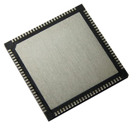
 Irvine California, USA – TopLine now produces very large size 12x12mm Daisy Chain QFN components with dummy silicon die for use in a variety of SMT process and thermal profile testing applications. These large-size, bottom terminal QFN packages feature 100 pins, spaced very fine pitch at 0.4mm. The package size conforms to JEDEC standards with package height not exceeding 1.0mm. The terminals and ground pads are plated with Nickel Palladium Gold (Ni Pd Au) to optimize SMT soldering.
The package level Daisy Chain circuit, made with 25µm gold bonding wire, forms an electrical connection between pads. These zero-ohm connections may be used to monitor electrical opens and shorts so that one may forensically determine the cause of PCB circuit board failure with simple GO/No-Go techniques using an ohm meter. Operating temperature range from -65⁰C to +150⁰C.
Other applications include PCB circuit board cleanliness testing incorporating S.I.R. Surface Insulation Resistance monitoring. For more information, visit www.topline.tv/DaisyChain.html


