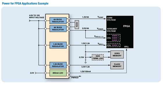
 The trend in medical and instrumentation devices, such as portable ultrasound and handheld instrumentation, is toward significantly smaller form factors, so these products are driving the need for smaller, more efficient ways of powering FPGAs, processors, and memory. A typical FPGA and memory design needs a very dense power supply that can deliver large currents with fast transient response to power the core and I/O rails, along with a low-noise rail to power on-chip analog circuitry such as a phase-locked loop (PLL). Power supply sequencing is critical to ensure that the FPGA is up and running before the memory is enabled. Regulators with a precision enable input and a dedicated power good output allow power supply sequencing and fault monitoring. Power supply designers often want to use the same power IC in different applications, so the ability to change the current limits is important. This design reuse can significantly reduce time to market—a critical element in any new product development process.
Consider a common multi-rail power management design specification for anFPGA with a 12-V input and five outputs:
- Core: 1.2V @ 4 A
- Auxiliary: 1.8V @ 4 A
- I/O: 3.3V @ 1.2A
- DDR memory: 1.5V @ 1.2A
- Clock: 1.0V @ 200mA
A typical discrete implementation connects four switching regulators to the 12-V input rail. The output of one switching regulator pre-regulates the LDO to reduce power dissipation. An alternative approach uses one regulator to step the 12-V input down to a 5-V intermediate rail, which is then regulated down to produce each of the required voltages. This implementation has a lower solution cost, but also a lower efficiency due to the two-stage power conversion. In both cases, each regulator has to be enabled independently, so supply sequencing may require a dedicated power supply sequencer. Noise may also be an issue, unless all of the switchers can be synchronized to reduce beat frequencies.
Integrating multiple buck regulators and LDOs into a single package can reduce the overall size of a power management design. In addition, smart integrated solutions provide many advantages over traditional discrete implementations. Reducing the number of discrete components can significantly reduce the cost, complexity, and manufacturing cost of the design. The ADP505xfamily of integrated power management units (PMUs) can implement all these voltages and features in a single IC, using significantlyless PCB area and fewer components.
For highest efficiency, each of the buck regulators can be powered directly from 12V, removing the need for apre-regulator stage. Buck 1 and Buck 2 have programmable current limits (4A, 2.5A, or 1.2A), allowing the power supply designer to quickly and easy change the currents for new designs and significantly reducing the development time.The LDO can be powered from one of the buck regulators to provide a low-noise 1‑V rail for the noise-sensitive analog circuitry.
In some designs it is desirable to have both: a lower switching frequency to provide the highest power efficiency for the higher current rails; and a higher switching frequency to reduce inductor size and minimize PCB area for the lower current rails. A divide-by-2 option on the master switching frequency allows the ADP5050 to operate at two frequencies. The switching frequency forBuck 1 and Buck 3 can be set, via the I2C port, to one-half of the master switching frequency.
Author
Maurice O’Brien aurice.obrien@analog.com] joined Analog Devices in 2002, following his graduation from the University of Limerick, Ireland, with a Bachelor of Electronic Engineering. He currently works as a product marketing manager in the Power Management product line. In his spare time, Maurice enjoys horse riding, outdoor sports, and travel.


