Electronics Maker provides electronics news and updates from electronics industries, technologies field where reader can get latest news about electronics sector & technology.
- Q3 net revenues $3.19 billion; gross margin 33.2%; operating income of $180 million, including $37 million related to impairment, restructuring charges and other related phase-out costs; net income of $237 million
- Business outlook at mid-point: Q4 net revenues of $3.28 billion and gross margin of 35.0%
- “Q3 net revenues came slightly above the mid-point of our business outlook range, with higher revenues in Personal Electronics, while Automotive and Industrial performed as anticipated, and CECP was broadly in line with expectations. Gross margin was slightly below the mid-point of our business outlook range mainly due to product mix within Automotive and Industrial.”
- “On a year-over-year basis, Q3 net revenues decreased 2.0%, non-U.S. GAAP1 operating margin decreased to 6.8% from 11.7% and non-U.S. GAAP1 net income decreased to $267 million from $351 million.”
- “In the third quarter, our book-to-bill ratio was above one, with Automotive above parity and Industrial at parity.”
- “Our fourth quarter business outlook, at the mid-point, is for net revenues of $3.28 billion, increasing sequentially by 2.9%, gross margin is expected to be about 35.0%; including about 290 basis points of unused capacity charges.”
- “The mid-point of this outlook translates into full year 2025 revenues of about $11.75 billion. This represents a 22.4% growth in the second half compared to the first half, confirming signs of market recovery. Gross margin is expected to be about 33.8%.”
- To optimize our investments in response to the current market conditions, we have reduced our Net Capex plan, now slightly below $2 billion for FY25.”
- “Our strategic priorities remain clear: accelerating innovation; executing our company-wide program to reshape our manufacturing footprint and resize our global cost base, which remains on schedule to deliver the targeted savings; and strengthening free cash flow generation.”
- Revenue increased 7.0% mainly due to Imaging.
- Operating profit increased by 2.1% to $221 million. Operating margin was 15.4% compared to 16.1%.
- Revenue decreased 34.3%.
- Operating profit decreased from $80 million to an operating loss of $67 million. Operating margin was -15.6% compared to 12.2%.
- Revenue increased 8.7% mainly due to General Purpose MCU.
- Operating profit increased by 9.4% to $161 million. Operating margin was 16.5% compared to 16.4%.
- Revenue decreased 3.4%.
- Operating profit decreased by 31.6% to $57 million. Operating margin was 16.6% compared to 23.4%.
- Net revenues are expected to be $3.28 billion, an increase of 2.9% sequentially, plus or minus 350 basis points.
- Gross margin of 35.0%, plus or minus 200 basis points.
- This outlook is based on an assumed effective currency exchange rate of approximately $1.15 = €1.00 for the 2025 fourth quarter and includes the impact of existing hedging contracts.
- The fourth quarter will close on December 31, 2025.
- changes in global trade policies, including the adoption and expansion of tariffs and trade barriers, that could affect the macro-economic environment and directly or indirectly adversely impact the demand for our products;
- uncertain macro-economic and industry trends (such as inflation and fluctuations in supply chains), which may impact production capacity and end-market demand for our products;
- customer demand that differs from projections which may require us to undertake transformation measures that may not be successful in realizing the expected benefits in full or at all;
- the ability to design, manufacture and sell innovative products in a rapidly changing technological environment;
- changes in economic, social, public health, labor, political, or infrastructure conditions in the locations where we, our customers, or our suppliers operate, including as a result of macro-economic or regional events, geopolitical and military conflicts, social unrest, labor actions, or terrorist activities;
- unanticipated events or circumstances, which may impact our ability to execute our plans and/or meet the objectives of our R&D and manufacturing programs, which benefit from public funding;
- financial difficulties with any of our major distributors or significant curtailment of purchases by key customers;
- the loading, product mix, and manufacturing performance of our production facilities and/or our required volume to fulfill capacity reserved with suppliers or third-party manufacturing providers;
- availability and costs of equipment, raw materials, utilities, third-party manufacturing services and technology, or other supplies required by our operations (including increasing costs resulting from inflation);
- the functionalities and performance of our IT systems, which are subject to cybersecurity threats and which support our critical operational activities including manufacturing, finance and sales, and any breaches of our IT systems or those of our customers, suppliers, partners and providers of third-party licensed technology;
- theft, loss, or misuse of personal data about our employees, customers, or other third parties, and breaches of data privacy legislation;
- the impact of IP claims by our competitors or other third parties, and our ability to obtain required licenses on reasonable terms and conditions;
- changes in our overall tax position as a result of changes in tax rules, new or revised legislation, the outcome of tax audits or changes in international tax treaties which may impact our results of operations as well as our ability to accurately estimate tax credits, benefits, deductions and provisions and to realize deferred tax assets;
- variations in the foreign exchange markets and, more particularly, the U.S. dollar exchange rate as compared to the Euro and the other major currencies we use for our operations;
- the outcome of ongoing litigation as well as the impact of any new litigation to which we may become a defendant;
- product liability or warranty claims, claims based on epidemic or delivery failure, or other claims relating to our products, or recalls by our customers for products containing our parts;
- natural events such as severe weather, earthquakes, tsunamis, volcano eruptions or other acts of nature, the effects of climate change, health risks and epidemics or pandemics in locations where we, our customers or our suppliers operate;
- increased regulation and initiatives in our industry, including those concerning climate change and sustainability matters and our goal to become carbon neutral in all direct and indirect emissions (scopes 1 and 2), product transportation, business travel, and employee commuting emissions (our scope 3 focus), and to achieve our 100% renewable electricity sourcing goal by the end of 2027;
- epidemics or pandemics, which may negatively impact the global economy in a significant manner for an extended period of time, and could also materially adversely affect our business and operating results;
- industry changes resulting from vertical and horizontal consolidation among our suppliers, competitors, and customers;
- the ability to successfully ramp up new programs that could be impacted by factors beyond our control, including the availability of critical third-party components and performance of subcontractors in line with our expectations; and
- Four new 5MP image sensors allow customers to optimize image capture with high speed, high detail with a single, flexible product instead of two chips
- New device family is ideal for high-speed automated manufacturing processes and object tracking
- New sensors leverage market-leading technology for both global and rolling shutter modes, with a compact 2.25µm pixel with advanced 3D stacking, and on-chip RGB-IR separation
- Designed, built, owned, and operated by a joint venture between SP Group and Daikin Airconditioning (Singapore), the innovative district cooling system will significantly improve the environmental performance of ST’s high-volume semiconductor manufacturing site in Singapore
- New system expected to reduce carbon emissions by 120,000 tonnes per year, cooling-related electricity costs by 20 percent each year, and repurposing over half a million cubic meters of water consumption per year
The Rise of Electric Vehicles: Industry Growth, Charging Expansion, and Energy Trends
The automotive industry is undergoing a profound transformation as electric vehicles (EVs) gain traction worldwide. This shift is driven by technological advancements, environmental concerns, and changing consumer preferences. This article examines the growth of the electric vehicle industry, the expansion of charging infrastructure, and emerging energy trends.
Industry Growth
The electric vehicle market has witnessed remarkable growth over the past decade, with technological innovations paving the way for more efficient and affordable models. As battery technology advances, the cost of electric vehicles continues to decline, making them more accessible to the average consumer. The continuous improvement in production processes and economies of scale contribute significantly to this positive trend.
Global economic pressures have also accelerated the shift towards electric mobility, with governments offering incentives and subsidies to promote sales. A significant factor in this growth is the anticipated expansion of the electric vehicle charging station market, projected to reach an astonishing $225.9 billion by 2030. This influx of investment is poised to support the widespread adoption of electric transportation.
As of recent trends, there is a noticeable decline in the cost of fuel cells, highlighting the effects of technological advancement and enhanced operational efficiency. The battery prices have plunged by a substantial 80% over the last six years, creating an ideal environment for a surge in the sales of electric-powered golf carts, further broadening the scope of electric vehicle applications.
Charging Expansion
Charging infrastructure is a crucial component of the electric mobility ecosystem, and its expansion is imperative for supporting the growing fleet of electric vehicles. Currently, efforts are concentrated on expanding public and private charging networks to address range anxiety and facilitate longer trips. The development of fast-charging technologies represents a major advancement, significantly reducing the time required to recharge EV batteries.
Public-private partnerships are playing a vital role in the development of comprehensive charging networks. By collaborating with local governments and energy providers, private companies are paving the way for extensive, reliable, and efficient charging solutions. These partnerships ensure that charging stations are strategically placed along major travel routes and within city centers, enhancing convenience for EV drivers.
The expansion of charging infrastructure is crucial not only for personal vehicles but also for public transportation and freight services. Increasing the availability of charging stations encourages the adoption of electric buses and trucks, which are essential for reducing emissions in densely populated areas. Moreover, advancements in charging technology, such as wireless charging and ultra-fast chargers, promise to revolutionize the refueling process, making it as quick and convenient as traditional fuel stations.
Energy Trends
The shift to electric vehicles is intrinsically linked to broader energy trends, including renewable energy integration and grid adaptation. As more vehicles transition to electric, the demand for clean and sustainable energy sources amplifies. Consequently, there is a significant push towards incorporating wind, solar, and other renewables into the energy grid.
The International Energy Agency (IEA) projects that electricity consumption will experience robust growth, rising by an estimated 4.3% in 2024 compared to 2.5% in 2023. This trend underscores the necessity for scalable and flexible energy systems capable of meeting surging demand. Advanced smart grid technologies are essential for efficient load management and energy distribution, ensuring that the growing fleet of electric vehicles is sustainably supported.
The integration of vehicle-to-grid (V2G) systems further exemplifies the potential of electric vehicles to contribute to energy resilience. By allowing stored energy in EVs to be fed back into the grid, these systems offer a dynamic solution for balancing energy supply and demand. This innovative approach not only supports grid stability but also provides financial incentives for EV owners, positioning electric vehicles as both a transportation solution and an energy asset.
The rise of electric vehicles represents a paradigm shift in how we approach transportation and energy consumption. Through continuous innovation, supportive policies, and strategic infrastructure development, the electric vehicle industry is paving the way towards a more sustainable future. As technology advances and energy trends align, the future of mobility looks increasingly electric, promising cleaner air and reduced reliance on fossil fuels.
Read moreStaying Safe and Sustainable With Home Technology
In today's world, technology has become an integral part of our daily lives, offering both convenience and efficiency. As we embrace these advancements, it is crucial to ensure that we are adopting technologies that are not only safe but also sustainable. From reducing our carbon footprint to enhancing security, home technology can play a significant role in achieving these goals.
Embracing Renewable Energy with Solar Technology
One of the most impactful ways to promote sustainability in our homes is through the use of solar energy. By turning to solar power, homeowners can significantly decrease their dependency on fossil fuels. According to Chariot Energy, users of solar energy can prevent around 35 tons of carbon dioxide emissions and save the equivalent of 75 million barrels of oil each year.
Installing solar panels can also lead to substantial savings on energy bills. This technology harnesses the abundant and renewable power of the sun, converting it into electricity for home use. As a result, households become more self-sufficient and less reliant on traditional power sources, leading to both environmental and economic advantages.
Moreover, the integration of solar technology can enhance property value. As more individuals recognize the benefits of sustainable energy, homes equipped with solar panels are increasingly attractive in real estate markets. This not only contributes to energy efficiency but also serves as a future-proof investment for homeowners.
Enhancing Home Security with Smart Technology
Adopting smart technology in home security is another way to ensure safety while embracing innovation. According to Yankee Security, the demand for electronic or digital locks is rapidly increasing, accounting for about 30% of locksmiths' tasks. This burgeoning trend in smart home technology has been growing by an impressive 15% annually, further highlighting its popularity and usefulness.
Smart locks provide homeowners with convenient and secure access to their properties. By utilizing codes, biometric recognition, or mobile devices, residents can control entry points with ease and confidence. This eliminates the need for traditional keys, reducing the risk of unauthorized access or key loss.
With advancements in technology, these smart security systems can even be integrated with home automation devices. This integration enables remote monitoring and alerts, offering peace of mind whether you are at home or away. As technology continues to evolve, its role in home security will likely expand, providing even more reliable and effective solutions.
Maintaining Health and Hygiene in Technological Spaces
As we integrate technology into our homes, maintaining hygiene in these spaces becomes increasingly important. According to the National Center for Health Research, office keyboards, for example, can become breeding grounds for bacteria, harboring up to 7,500 bacteria per square inch. This highlights the need for cleanliness, particularly in home offices where technology is frequently utilized.
Regular cleaning of technological devices is crucial to sustaining a healthy environment. With the use of antibacterial cleaners and wipes, homeowners can keep their gadgets germ-free. Ensuring that touchpoints are sanitized reduces the risk of illnesses and contributes to overall well-being.
Furthermore, innovations such as touchless technology can further promote health and hygiene in homes. Eliminating the need for direct contact with devices helps minimize the spread of germs. As we continue to innovate, creating healthier living environments complements the convenience of modern technology.
Integrating safe and sustainable technology in our homes is essential for promoting environmental conservation, enhancing security, and maintaining hygiene. Solar energy systems cut down carbon emissions significantly, while smart locks provide robust security measures. Additionally, maintaining cleanliness in our technologically-enhanced spaces is imperative for health.
Ultimately, embracing technology responsibly can significantly benefit both the planet and our immediate environments. As we advance, continuously evaluating the impact of technology on safety, sustainability, and health is imperative. By doing so, we fortify our homes for the future while minimizing our ecological footprint.
Read moreIncorporating Technological Comforts Into Your Home
Technology has become an integral part of our daily lives, changing not just how we work and communicate but also how we create and enjoy comfort in our homes. The modern home is evolving to accommodate new tech that promises to make life easier, more efficient, and incredibly convenient. From energy-efficient lighting to smart kitchen devices and automated systems for lawn care, incorporating these technological advances can enhance both the value and livability of your home.
Lighting Up Your Home Efficiently
One of the simplest ways to modernize your home is by upgrading to energy-efficient lighting. Light-emitting diodes, commonly known as LEDs, are a remarkable advancement in home lighting technology. Utilizing up to 90% less energy than traditional incandescent bulbs and lasting as long as 25 times more, LEDs are not only more efficient but also cost-effective over their lifespan.
Beyond their efficiency, LEDs provide a variety of lighting options that can transform the ambiance of your home. With options for color changes and adjustable intensities, they offer homeowners the ability to tailor their lighting schemes to match different moods and occasions. The initial investment in LED lighting can be quickly recouped through savings on your energy bill.
Installing smart lighting systems can further enhance efficiency and convenience. These systems can be controlled remotely using smartphone apps or voice commands, allowing homeowners to adjust lighting from anywhere. This integration of technology into your home not only saves on energy costs but also provides enhanced security options by automating lighting schedules.
The Smart Kitchen Revolution
The heart of the modern home, the kitchen, is undergoing its own tech transformation. Studies indicate that homeowners tend to remodel their kitchens approximately every 10 to 15 years, often incorporating new technology to improve both aesthetics and functionality. With the introduction of smart appliances, from refrigerators that manage your grocery inventory to ovens you can preheat remotely, the kitchen has never been more digitally enabled.
Introducing technology into the kitchen isn't just about efficiency; it's about ensuring a healthier and more environmentally friendly approach to food preparation. Smart appliances can help in reducing energy consumption through optimal performance, and with features such as precise temperature control, they help in preserving the nutritional quality of cooked foods.
Moreover, voice assistant technology, which integrates seamlessly with many smart kitchen gadgets, further enhances the cooking experience. From setting timers to searching recipes hands-free, these digital assistants make multitasking in the kitchen a breeze. As technology continues to evolve, the kitchen remains at the forefront of home innovation, blending comfort and convenience for a modern culinary experience.
Streamlining Home Maintenance with Technology
Technology also plays a crucial role in easing the burden of home maintenance, particularly in outdoor spaces. With approximately 20% of American homes equipped with automatic irrigation systems, according to the Environmental Protection Agency, many homeowners are turning to technology to care for their lawns more efficiently. These systems can be optimized to reduce water consumption and ensure your landscaping remains lush and vibrant throughout the seasons.
Smart irrigation systems take it a step further by using weather data and smart sensors to adjust watering schedules automatically, preventing over-watering and conserving precious resources. As environmental concerns grow, investing in a technologically advanced irrigation system can provide peace of mind and financial savings. Furthermore, it reflects a commitment to sustainable living practices, which is increasingly important in modern society.
Other home maintenance technologies include robotic lawn mowers and gutter-cleaning devices, which allow homeowners to dedicate less time to tedious outdoor chores. These innovations not only save time but also reduce the physical labor involved in home upkeep tasks.
Incorporating technological comforts into your home is not just a luxury but a strategic move towards enhancing quality of life. From smart lighting and kitchen appliances to advanced home maintenance systems, the adoption of technology can transform your living space into a more comfortable, efficient, and sustainable environment. Embracing these innovations ensures that your home remains a modern haven in a rapidly changing world.
Read moreIs It Time to Invest In Home Solar Panels?
With rising energy costs and a growing emphasis on sustainability, many homeowners are considering the switch to solar energy. Home solar panels offer a cleaner and potentially more cost-effective way of powering your home. However, before making such a significant investment, it's essential to understand the benefits and implications of installing solar panels.
The decision to invest in solar technology is not just about environmental consciousness; it’s also about economic practicality and future-proofing. As advanced tech continues to evolve, solar panels have become more efficient and affordable. In this article, we will explore the financial incentives, efficiency improvements, and longevity of solar panels to help you decide if now is the right time to make the switch.
Financial Incentives for Solar Panel Installation
One of the most compelling reasons to consider investing in solar panels is the array of financial incentives available. According to Energy Sage, you can offset nearly one-third of your solar installation costs due to federal tax credits. This significant tax deduction can make the initial cost of installing solar panels much more manageable for many households.
In addition to federal tax incentives, many states and utility companies offer rebates and additional credits for solar systems. These programs are designed to encourage more homeowners to transition to renewable energy by further reducing the financial barriers. When combined with the federal tax deductions, these local incentives can significantly lower the overall cost of your solar installation.
The long-term financial benefits of solar energy extend beyond the initial installation cost reductions. Once installed, solar panels can lead to substantial savings on your monthly electricity bills. Over time, this reduced dependency on traditional power sources can help you save thousands of dollars, effectively paying for the solar system itself.
Efficiency and Technological Advancements in Solar Panels
The efficiency of solar panels has significantly improved over the years, thanks to advancements in tech. Most commercial solar panels now boast efficiencies between 19.7% and 21.6%, with premium options reaching close to 23%, as reported by Consumer Affairs. This means that more solar energy can be converted into usable electricity, making modern solar panels much more efficient than those of previous generations.
These efficiency gains are a result of both material advancements and innovative design improvements in solar technology. Researchers and solar manufacturers continually work to optimize the performance of solar cells, ensuring they can harness more sunlight even in less-than-optimal conditions. This progress has led to increasingly efficient solar panels, which are now capable of delivering more consistent energy output throughout the day and year.
Moreover, the tech behind solar installations has evolved to include better inverters, battery storage, and smart home integration. These advancements allow homeowners not only to generate more power but also to store excess energy for use during peak times or outages. Integrated solar systems can now collaborate with smart home devices, optimizing energy use and further enhancing overall system efficiency.
Longevity and Durability of Solar Systems
When considering the investment in solar technology, it’s important to factor in the lifespan and maintenance of the system. As per Solar Power Authority, a typical solar roof will maintain peak performance for around 20 years. This means that once installed, the system can reliably produce energy for two decades, providing a consistent return on investment.
The durability of solar panels has improved significantly, thanks to better manufacturing processes and materials. Modern panels are designed to withstand various weather conditions, including heavy rain, high winds, and even snowfall. This robustness means you can expect a long-lasting energy solution that requires minimal maintenance over its lifespan.
In addition to the longevity of the solar panels themselves, many manufacturers offer warranties that cover up to 25 years. These warranties not only provide peace of mind but also demonstrate the confidence manufacturers have in their products. By investing in solar energy today, you can secure a reliable power source that will serve you well into the future.
Ultimately, the choice to install solar panels is a commitment to innovation and responsibility. As we continue to witness the impacts of climate change, transitioning to solar energy becomes not only a wise financial decision but also a vital contribution to global sustainability efforts. The time to embrace solar power is now.
Read moreSTMicroelectronics Reports 2025 Third Quarter Financial Results
Geneva, October 23, 2025 – STMicroelectronics N.V. (“ST”) (NYSE: STM), a global semiconductor leader serving customers across the spectrum of electronics applications, reported U.S. GAAP financial results for the third quarter ended September 27, 2025. This press release also contains non-U.S. GAAP measures (see Appendix for additional information).
ST reported third quarter net revenues of $3.19 billion, gross margin of 33.2%, operating income of $180 million, and net income of $237 million or $0.26 diluted earnings per share (non-U.S. GAAP1 operating income of $217 million, and non-U.S. GAAP1 net income of $267 million or $0.29 diluted earnings per share).
Jean-Marc Chery, ST President & CEO, commented:
Quarterly Financial Summary
| U.S. GAAP(US$ m, except per share data) | Q3 2025 | Q2 2025 | Q3 2024 | Q/Q | Y/Y |
| Net Revenues | $3,187 | $2,766 | $3,251 | 15.2% | -2.0% |
| Gross Profit | $1,059 | $926 | $1,228 | 14.3% | -13.7% |
| Gross Margin | 33.2% | 33.5% | 37.8% | -30 bps | -460 bps |
| Operating Income (Loss) | $180 | $(133) | $381 | - | -52.9% |
| Operating Margin | 5.6% | -4.8% | 11.7% | 1,040 bps | -610 bps |
| Net Income (Loss) | $237 | $(97) | $351 | - | -32.3% |
| Diluted Earnings Per Share | $0.26 | $(0.11) | $0.37 | - | -29.7% |
| Non-U.S. GAAP1(US$ m, except per share data) | Q3 2025 | Q2 2025 | Q3 2024 | Q/Q | Y/Y |
| Operating Income | $217 | $57 | $381 | 278.8% | -43.2% |
| Operating Margin | 6.8% | 2.1% | 11.7% | 470 bps | -490 bps |
| Net Income | $267 | $57 | $351 | 369.1% | -23.9% |
| Diluted Earnings Per Share | $0.29 | $0.06 | $0.37 | 383.3% | -21.6% |
Third Quarter 2025 Summary Review
Reminder: on January 1, 2025, we made some adjustments to our segment reporting. Prior year comparative periods have been adjusted accordingly. See Appendix for more detail.
| Net Revenues by Reportable Segment2(US$ m) | Q3 2025 | Q2 2025 | Q3 2024 | Q/Q | Y/Y |
| Analog products, MEMS and Sensors (AM&S) segment | 1,434 | 1,133 | 1,340 | 26.6% | 7.0% |
| Power and discrete products (P&D) segment | 429 | 447 | 652 | -4.3% | -34.3% |
| Subtotal: Analog, Power & Discrete, MEMS and Sensors (APMS) Product Group | 1,863 | 1,580 | 1,992 | 17.9% | -6.5% |
| Embedded Processing (EMP) segment | 976 | 847 | 898 | 15.3% | 8.7% |
| RF & Optical Communications (RF&OC) segment | 345 | 336 | 357 | 2.4% | -3.4% |
| Subtotal: Microcontrollers, Digital ICs and RF products (MDRF) Product Group | 1,321 | 1,183 | 1,255 | 11.6% | 5.3% |
| Others | 3 | 3 | 4 | - | - |
| Total Net Revenues | $3,187 | $2,766 | $3,251 | 15.2% | -2.0% |
Net revenues totaled $3.19 billion, representing a year-over-year decrease of 2.0%. Year-over-year net sales to OEMs and Distribution decreased 5.1% and increased 7.6%, respectively. On a sequential basis, net revenues increased 15.2%, 60 basis points better than the mid-point of ST’s guidance.
Gross profit totaled $1.06 billion, representing a year-over-year decrease of 13.7%. Gross margin of 33.2%, 30 basis points below the mid-point of ST’s guidance, decreased 460 basis points year-over-year, mainly due to lower manufacturing efficiencies, negative currency effect, lower level of capacity reservation fees and, to a lesser extent, the combination of sale price and product mix.
Operating income decreased from $381 million in the year-ago quarter to $180 million. ST’s operating margin decreased 610 basis points on a year-over-year basis to 5.6% of net revenues, compared to 11.7% in the third quarter of 2024. Operating income included $37 million impairment, restructuring charges and other related phase-out costs for the quarter, reflecting impairment of assets and restructuring charges predominantly associated with the previously announced company-wide program to reshape our manufacturing footprint and resize our global cost base. Excluding these items, non-U.S. GAAP1 Operating income stood at $217 million in the third quarter.
By reportable segment, compared with the year-ago quarter:
In Analog, Power & Discrete, MEMS and Sensors (APMS) Product Group:
Analog products, MEMS and Sensors (AM&S) segment:
Power and Discrete products (P&D) segment:
In Microcontrollers, Digital ICs and RF products (MDRF) Product Group:
Embedded Processing (EMP) segment:
RF & Optical Communications (RF&OC) segment:
Net Earnings and diluted Earnings Per Share decreased to $237 million and $0.26 respectively, compared to $351 million and $0.37 respectively in the year-ago quarter. Non-U.S. GAAP1 Net income and diluted Earnings Per Share, stood at $267 million and $0.29 respectively in the third quarter of 2025.
Cash Flow and Balance Sheet Highlights
| Trailing 12 Months | ||||||
| (US$ m) | Q3 2025 | Q2 2025 | Q3 2024 | Q3 2025 | Q3 2024 | TTM Change |
| Net cash from operating activities | 549 | 354 | 723 | 2,158 | 3,764 | -42.7% |
| Free cash flow (non-U.S. GAAP1) | 130 | (152) | 136 | 136 | 813 | -83.3% |
Net cash from operating activities was $549 million in the third quarter compared to $723 million in the year-ago quarter.
Net Capex (non-U.S. GAAP1), was $401 million in the third quarter compared to $565 million in the year-ago quarter.
Free cash flow (non-U.S. GAAP1) was positive $130 million in the third quarter, compared to positive $136 million in the year-ago quarter.
Inventory at the end of the third quarter was $3.17 billion, compared to $3.27 billion in the previous quarter and $2.88 billion in the year-ago quarter. Days sales of inventory at quarter-end was 135 days, compared to 166 days for the previous quarter and 130 days for the year-ago quarter.
In the third quarter, ST paid cash dividends to its stockholders totaling $81 million and executed a $91 million share buy-back, as part of its current share repurchase program.
ST’s net financial position (non-U.S. GAAP4) remained strong at $2.61 billion as of September 27, 2025, compared to $2.67 billion as of June 28, 2025, and reflected total liquidity2 of $4.78 billion and total financial debt of $2.17 billion. Adjusted net financial position (non-U.S. GAAP1), taking into consideration the effect on total liquidity of advances from capital grants for which capital expenditures have not been incurred yet, stood at $2.27 billion as of September 27, 2025.
Corporate developments
On July 24, 2025, ST entered into a definitive transaction agreement for the acquisition of NXP’s MEMS sensor business for a purchase price of up to $950 million in cash, including $900 million upfront and $50 million subject to the achievement of technical milestones. The transaction which will be financed with existing liquidity is subject to customary closing conditions, including regulatory approvals, and is expected to close in H1 2026.
Business Outlook
ST’s guidance, at the mid-point, for the 2025 fourth quarter is:
This business outlook does not include any impact of potential further changes to global trade tariffs compared to the current situation.
Conference Call and Webcast Information
ST will conduct a conference call with analysts, investors and reporters to discuss its third quarter 2025 financial results and current business outlook today at 9:30 a.m. Central European Time (CET) / 3:30 a.m. U.S. Eastern Time (ET). A live webcast (listen-only mode) of the conference call will be accessible at ST’s website, https://investors.st.com, and will be available for replay until November 7, 2025.
Use of Supplemental Non-U.S. GAAP Financial Information
This press release contains supplemental non-U.S. GAAP financial information.
Readers are cautioned that these measures are unaudited and not prepared in accordance with U.S. GAAP and should not be considered as a substitute for U.S. GAAP financial measures. In addition, such non-U.S. GAAP financial measures may not be comparable to similarly titled information from other companies. To compensate for these limitations, the supplemental non-U.S. GAAP financial information should not be read in isolation, but only in conjunction with ST’s consolidated financial statements prepared in accordance with U.S. GAAP.
See the Appendix of this press release for a reconciliation of ST’s non-U.S. GAAP financial measures to their corresponding U.S. GAAP financial measures.
Forward-looking Information
Some of the statements contained in this release that are not historical facts are statements of future expectations and other forward-looking statements (within the meaning of Section 27A of the Securities Act of 1933 or Section 21E of the Securities Exchange Act of 1934, each as amended) that are based on management’s current views and assumptions, and are conditioned upon and also involve known and unknown risks and uncertainties that could cause actual results, performance or events to differ materially from those anticipated by such statements due to, among other factors:
ST introduces new image sensors for industrial automation, security and retail applications

STMicroelectronics (NYSE: STM), a global semiconductor leader serving customers across the spectrum of electronics applications, introduces a new family of 5MP CMOS image sensors: VD1943, VB1943, VD5943, and VB5943. These advanced ST BrightSense sensors are designed to accelerate the development of innovative vision applications across industries, including advanced industrial automation with enhanced machine and robotic vision, next-generation security including biometric identification and traffic management, and smart retail applications such as inventory management and automated checkout. A longtime leader in optical sensing technology for consumer applications, ST continues to expand its offering for new applications with its industry-leading design, 3D stacking expertise and high-volume manufacturing for market-leading performance.
“Our new image sensors with hybrid global and rolling shutter modes allow our customers to optimize image capture, ensuring motion-artifact-free video capture and low-noise, high-detail imaging at the same time, making it ideal for high-speed automated manufacturing processes and object tracking. This architecture is unique on market today and provides unmatched flexibility, performance, and integration. We continue to broaden our portfolio of solutions for a wide range of industrial applications and want to bring the best of optical sensing technologies to both existing and new applications,” said Alexandre Balmefrezol, Executive Vice President and General Manager of STMicroelectronics’s Imaging Sub-Group.
"Industrial and security imaging are pushing sensor performance to new levels, enabling functions from identification to robotic guidance, gauging and advanced monitoring and inspection,” said Florian Domengie, PhD Principal Analyst Imaging at Yole Group. “By 2030, this image sensor market is projected to reach $3.9 billion with over 500 million units shipped. Key advances will include enhanced low-light performance, on-chip intelligence, and hybrid global/rolling shutter operation, combining low noise with high-precision temporal sensing."*
*Source: Status of the CMOS Image Sensor Industry 2025 – 3D Imaging & Sensing 2025, Yole Group
Technical notes
The VD1943, VD5943, VB1943, and VB5943 sensors, part of the ST BrightSense portfolio, are ready for evaluation and sampling, with mass production scheduled to begin in February 2026. Detailed documentation, evaluation kits, and product samples, are available through the local ST sales representative or an authorized distributor.
| Product code | Chroma | Package |
| VD5943 | Monochrome | Sensor die |
| VB5943 | Monochrome | OBGA sensor |
| VD1943 | RGB-IR | Sensor die |
| VB1943 | RGB-IR | OBGA sensor |
Dual global and rolling shutter modes
The sensors provide hybrid global and rolling shutter modes, allowing developers to optimize image capture for specific application requirements. This functionality ensures motion-artifact-free video capture (global shutter) and low-noise, high-detail imaging (rolling shutter), making it ideal for high-speed object tracking and automated manufacturing processes.
Compact design with advanced pixel technology
Using 2.25 µm pixel technology and advanced 3D stacking, the sensors deliver high image quality in a smaller footprint. The die size is 5.76 mm by 4.46 mm, with a package size of 10.3 mm by 8.9 mm, and an industry-leading 73%-pixel array-to-die surface ratio. This compact design enables integration into space-constrained embedded vision systems without compromising performance.
On-chip RGB-IR separation
The RGB-IR variants of the sensors feature on-chip RGB-IR separation, eliminating the need for additional components and simplifying system design. This capability supports multiple output patterns, including 5MP RGB-NIR 4x4, 5MP RGB Bayer, 1.27MP NIR subsampling, and 5MP NIR smart upscale, with independent exposure times and instant output pattern switching. This integration reduces costs while maintaining full 5MP resolution for both color and infrared imaging.
Enhanced imaging performance
The sensors incorporate backside illumination (BSI) and capacitive deep trench isolation (CDTI) pixel technologies to enhance sensitivity and sharpness, particularly in low lighting conditions. Single-frame on-chip HDR improves detail visibility across bright and dark areas. These features enable high-quality imaging in challenging environments and support advanced machine vision and edge AI applications.
Read moreSingapore’s largest industrial district cooling system begins operationsto support STMicroelectronics’ decarbonization strategy
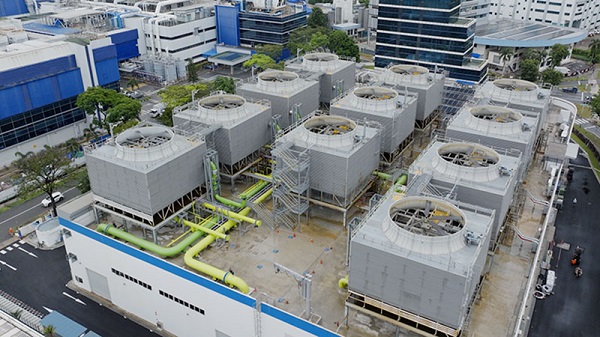
STMicroelectronics (NYSE: STM), a global semiconductor leader serving customers across the spectrum of electronics applications, and SP Group (SP), a leading utilities group in the Asia Pacific and Singapore’s national grid operator, have commenced operations for Singapore’s largest industrial district cooling system at STMicroelectronics’ (ST) Ang Mo Kio TechnoPark. The event was inaugurated by Ms. Low Yen Ling, Senior Minister of State, Ministry of Trade and Industry and Ministry of Culture, Community and Youth.
The system is expected to reduce carbon emissions by up to 120,000 tonnes per year and enable 20 per cent savings on cooling-related electricity consumption. It will also repurpose over half a million cubic meters of water each year by using reject reverse osmosis water, previously used in ST Cooling Towers, to support the new district cooling operations.
This marks ST’s first use of district cooling at a manufacturing facility and will strengthen ST’s commitment to be carbon neutral by 2027.
“The deployment of Singapore’s largest industrial district cooling system at our Ang Mo Kio TechnoPark demonstrates our commitment to pioneering energy-efficient solutions that reduce carbon emissions and conserve resources. This achievement strengthens our partnership with Singapore in advancing its national sustainability goals,” said Rajita D’Souza, President of Human Resources and Corporate Social Responsibility at STMicroelectronics. “By integrating advanced technologies like the district cooling system, we are driving a smarter, more sustainable future — showcasing how industry leadership and environmental stewardship align to create lasting value for our business, communities, and the planet.”
“SP Group’s strategic partnership with STMicroelectronics marks a pivotal milestone in our nation’s transition towards a low-carbon future. This project showcases how collaborative innovation can transform urban infrastructure to deliver sustainable, energy-efficient solutions. District cooling will continue to play a vital role in Singapore’s net-zero ambitions, enabling carbon emissions reduction and enhancing energy resilience across industrial and urban developments,” said Stanley Huang, SP’s Group Chief Executive Officer.
Technical information about the district cooling system
Designed, built, owned, and operated by a joint venture between SP and Daikin Airconditioning (Singapore), the system has an installed capacity of up to 36,000 refrigeration tonnes (RT). It delivers continuous chilled water to cool both manufacturing and office spaces via a centralized closed-loop pipe network replacing individual chillers in each building. The total area served by the system is approximately 90,000 square metres.
Chillers in series counterflow configuration reduce the energy required to cool the water. This ensures an efficient and reliable 24/7 operation, with remote monitoring capabilities augmenting the operations team on site to come.
“This partnership with SP reflects Daikin’s commitment to delivering advanced, energy-efficient solutions that go beyond immediate operational needs. Our goal is to contribute to a more sustainable built environment, where technology plays a key role in enhancing resilience, reducing environmental impact, and supporting Singapore’s long-term climate ambitions,” said Chua Ban Hong, Managing Director at Daikin Airconditioning (Singapore).
Additionally, the new installations free up around 4,000 square meters of space at Ang Mo Kio TechnoPark, which will enable ST to install other equipment contributing to environmental impact mitigation. This includes perfluorocarbon (PFC) abatement equipment, with near-future plans for additional water reclamation systems and volatile organic compounds (VOC) abatement as part of its ongoing sustainability efforts.
The project achieved over 2 million accident-free man hours, underscoring the commitment to safety during construction. The district cooling plant has been awarded the Green Mark Platinum Super Low Energy certification by the Building and Construction Authority for its exceptional energy efficiency and sustainable design. Incorporating whole-life carbon assessments during design and construction of the plant also enabled a reduction of about 44 percent in embodied carbon compared to industrial building benchmarks, achieved through optimized material choices and system design to further lower the plant’s carbon footprint.
Further collaboration between STMicroelectronics and SP Group
To accelerate its decarbonization roadmap, ST has also partnered with SP to upgrade the cooling system at its Toa Payoh site. Under a 20-year chilled-water-as-a-service agreement, SP will design, build, operate, and maintain a new high-efficiency chiller system, scheduled for completion by December 2025. The system will improve energy efficiency and aims to reduce carbon emissions by approximately 2,140 tonnes annually.
In addition to sustainable cooling solutions, STMicroelectronics and SP Group are implementing a range of sustainable technologies across ST’s Ang Mo Kio and Toa Payoh campuses.
This includes the deployment of the energy management information system (EMIS), comprising 2,400 smart electricity meters and multi-utility sensors. With SP’s smart metering infrastructure in place, ST can monitor its overall energy consumption – enabling data-driven decisions that enhance efficiency and sustainability.
SP has also implemented smart water meters that track water inflow to five of ST’s buildings. This provides ST with an accurate view of its water consumption, allowing the organization to enhance its critical wafer fabrication operations by ensuring greater water efficiency.
Together, the partnership delivers on a shared vision for a smarter, cleaner energy future through integrated digitalization and decarbonization at scale.
Read moreSTMicroelectronics announces timing for third quarter 2025 earnings release and conference call
STMicroelectronics (NYSE: STM), a global semiconductor leader serving customers across the spectrum of electronics applications, announced that it will release third quarter 2025 earnings before the opening of trading on the European Stock Exchanges on October 23, 2025.
The press release will be available immediately after the release on the Company’s website at www.st.com.
STMicroelectronics will conduct a conference call with analysts, investors and reporters to discuss its third quarter 2025 financial results and current business outlook on October 23, 2025 at 9:30 a.m. Central European Time (CET) / 3:30 a.m. U.S. Eastern Time (ET).
A live webcast (listen-only mode) of the conference call will be accessible at ST’s website, https://investors.st.com, and will be available for replay until November 7, 2025.
Read more