The method of selective soldering is growing in the medical, automotive and aerospace industries as the preferred process to solder selectively through-hole (TH) components on a mixed technology assembly. The reason for its popularity is the ability to solder SMT assemblies which would otherwise need to be hand soldered, or passed over a wave soldering machine, but with it brings inherent problems.
Selective soldering allows a manufacturer to automatically solder mixed technology assemblies; TH pins can be accurately soldered, working around delicate SMT packages and targeting only the though hole areas on the board. This promotes increased reliability as heating of sensitive components is minimised to isolated areas on the PCB, and therefore producing fewer defects and overall cost reduction. As with all soldering, flux plays a critical role in this process, both the flux chemical properties and its application must be considered before successful soldering can be achieved and field defects minimised.
The application of flux facilitates the soldering process and has the primary purpose to clean the components and surfaces that are to be soldered. To obtain a reliable soldered joint, all surfaces need to be clean of any impurities or oxides. Chemicals can be used prior to soldering, but due to the increased temperatures required to melt the solder ,re-oxidation can occur on the metallic surfaces. Flux is applied to overcome this problem and provides the cleaning actions required, promotes wetting and helps form high quality intermetallic bonds. On a conventional wave solder process, the entire assembly is generally fluxed, preheated and passed over the solder bath. With selective soldering, only the area to be soldered by the nozzle is normally fluxed, with drop-jet style technologies employed to accurately spray small amounts of flux onto the PCB.
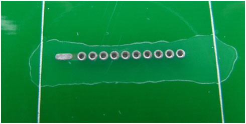
After discussions with both customers and machine manufacturers, the main problems reported in fluxing within the selective process were the need for verification of the X/Y positioning of the fluxer and detection of crystallisation build up in the nozzle resulting in flux being deposited in the wrong areas. This problem is twofold; insufficient fluxing of necessary components resulting in poor soldering, and additionally the potential of un-activated flux seeping under sensitive electronics, producing in-field failures.
In selective soldering the flux should not spread excessively as it is only required in the specific soldering area, if it spreads beyond the solder path to where there is no solder-washing action to remove it or insufficient heat to inactivate the flux, then the remaining flux can have detrimental effects on the PCB rendering them useless as the electronic function is affected.
Today many engineers are struggling to control the applied flux amounts. For good soldering more flux is sometimes needed. Applying more flux also results in potential risk that flux penetrates into surface mount device areas. To avoid this, it is important to understand properties of flux and printed circuit board.
The solder mask of the printed circuit board is a very important parameter that impacts the spreading of the flux alot. The flux spread depends on several factors including:
- Flux surface tension (flux type)
- Surface energy of the board (solder mask)
- Temperature of the flux
- Temperature of the board
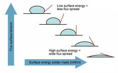
For wave soldering a board with a high surface energy (>50 mN/m) is preferred. This makes the flux spread to all areas and thus eliminates the risk for open solder joints, bridging, spikes and webbing. Due to the good spreading the residues will be less visible; which is a cosmetic advantage.
Non-activated flux residue is also a major risk for electro-migration causing problems with sensitive electronic circuits which often do not become apparent until the electronics are used in the field and conditions of the environment are brought into play. All flux formulas have components that require a sufficient heat cycle to become inactive, alternatively it must be washed away in a post-cleaning operation which in many applications is un-desirable. Because of the nature of the selective process, flux that has been mis-applied or has seeped under adjacent components may never see widespread heat unlike traditional wave or reflow soldering applications. Selective soldering has many advantages however for manufacturers but without correct control of all process elements it may pose new problems when it comes to fluxing.
With the need for selective soldering increasing, SolderStar has developed a dedicated range of process profiling products for the selective processes. One of the most advanced systems is the Wave Shuttle Selective device, it has been designed to analyse, improve and gain control of the mini-wave selective soldering process quickly. This instrument is unique due to it incorporating two measurement systems ensuring that the most comprehensive and repeatable measurement results are obtained.
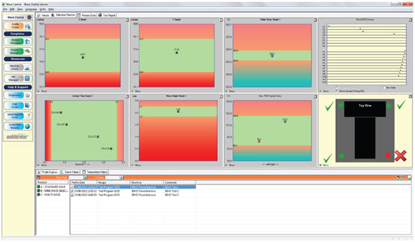
Using the unique Solderstar Smartlink system, it includes a dedicated measurement fixture/pallet. This includes three arrays of solder contact sensors, including;
- X Speed Sensor – which measure and verify the speed of the X axis of the machine
- Y Speed Sensor – which measure and verify the speed of the Y axis of the machine
- Height Array – Contact sensors that are set at height increments of to allow the height of the solder ‘bubble’ to verified
In addition to these innovations, a pre-heat temperature sensor and a solder temperature probe are added to verify all key parameters in a single pass. Uniquely it also incorporates a new flux measurement system which was developed after many months of intensive development and trials. Due to the many types of flux, which all perform differently, research into the universal problem of fluxing in the selective soldering process was a difficult problem to overcome, however SolderStar found a way to prevent the problems surrounding fluxing.
The final solution required a new sensor to be designed, manufactured from high temperature thermoplastics, with an embedded stainless steel surface resistance sensors. A new signal conditioning circuit was also developed providing a configurable measurement system which has the option to be trained on different flux compositions, which can detect flux spots of 2mm upwards, a real break-through in the detection of the small flux amounts applied during the selective soldering process. The new measurement sensors can be optionally installed to the measurement fixture, allowing for flux presence and position to be obtained as part of the daily production tests. All parameters can be quickly evaluated, with good and bad limits defined easily to allow periodic process verification to be performed without the need for specialist knowledge.
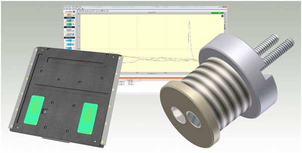
This optional addition to the selective soldering profiling range is benefitting companies worldwide, providing them with increased knowledge regarding machine capability and repeatability of the fluxing steps. Problems relating to crystallisation and fluxer alignment can be rectified quickly resulting in reduced failures and rework costs. This allows manufacturers to feel increasingly confident in their use of selective soldering in industries like the medical and aerospace worlds which demand the highest quality end product.


