The evolution to reconfigurable multipurpose radar, EW, and military communications systems to address tomorrow’s emerging threats is driving new system-level architectural and I/O requirements. In addition, supporting an increasingly networked infrastructure with high data throughput and low latency is becoming key for network- centric applications–all of which must be deployed faster and at a lower cost with today’s tightening budgets
 These trends are driving implementation changes from the system level down to digital components, including the digital interfaces that are used. Today’s systems increasingly rely on reconfigurable hardware such as field programmable gate arrays (FPGAs), digital signal processors (DSPs), and general-purpose processors (GPPs). High-speed I/O is needed to support high data rates between these devices, as well as memory, storage, and graphic processors/displays.
Here are the new demands that we’re seeing from the industry:
High speed (to real time) data reduction/analysis within the instrument (FPGA/DSP/GPU) – can no longer rely on instrument controller. Different processes and methodologies include:
- Digital down and up conversion (DDC/DUC)
- Real time meta data or pulse descriptiorword (PDW) generation from acquired raw data or generated algorithmically for playback (dynamic user control)
- Simultaneous high resolution time and frequency display (high sample rate and large FFT)
- Firmware defined measurement science
FPGA Test Challenges
With modern satellite, radar and EW architectures come a myriad of unique challenges, many of which emanate from the change in signal formats that happens through the transmitter and receiver.
Signal amplitudes once represented by an analogvoltage or potential between two points, are now a series of digital word sample points on a signal bus of many different voltage potentials. Often, the signal is represented on time sampled dual I–Q signal busses complicating test matters further.
Diagnosing digital issues thus requires a different test interface to different hardware. Probing IQ busses with many test connections become essential. Probing is often complicated when using FPGAs, as many of the desired test points may not be readily accessible outside of the chip.
To add to all these challenges, cross-format analysis is often a crucial troubleshooting need.
Since most satellite digital designs ultimately get converted back to analog signals, it is frequently necessary to compare the analog signal with the digital signal that initially created it. This requires cross-domain analysis capability to compare modulation parameters between a digital signal and an analog signal.
Keysight Test Solutions
In-Circuit FPGA Debug and Analysis Solution
With the advancement in the FPGA Technology, FPGAs have found application in most of the advanced Aerospace and Defense applications.
Now FPGAs are everywhere however debugging an FPGA-based system can be frustrating due to lack of adequate internal visibility. With bigger
FPGAs containing System-On-Chip(SoC) , which is very common nowadays, visibility becomes an even bigger challenge. A typical approach to have visibility inside the FPGA is to route the internal
FPGA nodes to a small number of dedicated physical pins that an instrument can measure. But this approach has some major challenges:
- Since pins on the FPGA are typically an expensive resource, there are a relatively small number available for debug. This limits internal visibility (i.e. one pin is required for each internal signal to be probed).
- When different internal signals need to be accessed you must change your design to route these signals to pins. This can be time consuming and can affect the timing of the FPGA design.
- Finally, the process required to map the signal names from the FPGA design to the logic analyzer setup is manual and tedious. When new signals are routed out, the need to manually update these signal names on the logic analyzer takes additional time and is a potential source of confusing error
With the FPGA Dynamic Probe Application the engineers can:
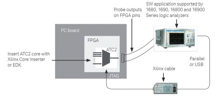
- View internal FPGA activity: With the FPGA dynamic probe, test engineers can now access signals internal to the FPGA with capability to measure up to 128 internal signals for each external pin dedicated to debug, unlocking more visibility into the design. Using an optional 2X time division compression in state mode, each pin can access 2 signals per bank.
- Move probe points internal to an FPGA: The FPGA Dynamic Probe application allows user to
Insert an ATC2 (Keysight Trace Core) core into their FPGA design. This helps engineers to measure different set of internal signals without design changes. The application makes sure that the FPGA timing stays constant even when new signals are selected for analysis.
- The FPGA dynamic probe is the industry’s first tool that maps internal signal names from your FPGA design tool to the logic analyzer
Author


