


The effective identification and debug of semiconductor issues is critical for the technical teams involved in system design and delivery. The challenging combination of increased system complexity and decreased time to market can result in extreme pressure on resolving issues in the shortest time possible – what engineer hasn’t been asked to deliver their fix yesterday? At time of such intense pressure, it can be difficult to follow a logical and structured approach in debugging an issue. Conversely though, following a logical and structured approach in debugging an issue is the very key to a timely resolution.
It is clear that a comprehensive debug framework could save engineers significant time and frustration in debugging complex semiconductor issues. Using illustrative examples, this article describes such a framework. Although video products are used as a lens to examine how semiconductor issues can manifest and be resolved, the framework outlined here should be considered as generic and applicable to many semiconductors and problems. Starting with the review of the application against any available reference schematics and layouts and culminating with the submission of parts through official failure analysis channels, this guide attempts to provide as comprehensive a framework as possible.
DON’T PANIC
 The front cover of the Hitchhiker’s Guide to the Galaxy [Adams, Douglas (1981), The Hitchhiker’s Guide to the Galaxy, New York: Pocket Books, 1981] famously called out a calming message to those who were lucky enough to possess a copy: Don’t Panic. Douglas Adam’s famously wrote that “despite its many glaring (and occasionally fatal) inaccuracies, the Hitchhiker’s Guide to the Galaxy itself has outsold the Encyclopedia Galactica because it is slightly cheaper, and because it has the words “DON’T PANIC” in large, friendly letters on the cover”.

We’ve all been there though. The demo system is overdue for delivery, the marketing department are on the phone looking for updates and a small group of engineers in the lab pours over a board which refuses to act as it was intended to. It is at times like this that an intergalactic traveller would reach for the Guide. Engineers have many alternatives to the Guide – the Internet, The Art of Electronics or even one of Dilbert’s many insightful cartoons. Such an exalted list is now augmented by this article – a fault-finding recipe that engineers can use to alleviate the panic when it occurs.
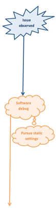
Start with software….
Every engineer has their own biases towards starting a debug with either software or hardware. Temporarily suppressing these biases (although the author does have a hardware background…), software can often be the best place to start a debug given the ability to change complex elements reasonably quickly and the sticky nature of hardware (e.g. the lead time involved in non-bill of materials changes).
Silicon vendors invest significant time and resources prior to releasing products to define optimal configuration settings which work across a range of operation conditions, such as process variations, temperature and voltage. Modern semiconductor devices such as HDMI receivers rely heavily on the use of optimal configuration settings to ensure their stable and robust operation. Although extra settings may need to be added to the core configuration settings to address application specific issues (e.g. input muxing, color space conversion), the core configuration settings must be maintained without adjustment.
When confronted with an issue, the configuration settings being employed in the application must be examined as a priority. If the configuration settings being employed do not match those recommended by the silicon vendor, the next step must be to change those settings before immediately retesting. The impact of incorrect settings can range from the slight (e.g. blurred video due to filters being disabled) to the serious (e.g. complete absence of video or failing compliance).
During software debug, it can be helpful to isolate a complex software driver with many interactions (e.g. interrupt responses, scheduled tasks) from the basic I2C configurations required for the system components. If everything works okay with the static configuration, the issue may be in the increased number of interactions incorporated into the software. If there are still issues, hardware debug is the next step.
Part To Play
Once software have been ruled out as the possible source for the issues being experienced, hardware is the next area for analysis. It might sound unlikely and elementary but the first stage of any hardware debug should be to confirm that the parts on the PCB are actually correct. Silicon vendors typically develop several models of each product with each model differentiated from the others in varying degrees.
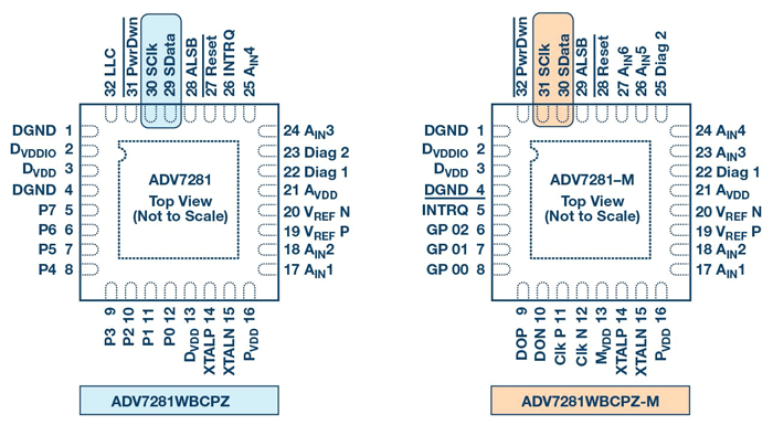
One common differentiator between models is in speed grade. A simple mistake in selecting from an ordering guide could result in a model which does not perform to the required specification e.g. an ADV7802BSTZ-150 video decoder operates at frequencies of up to 150MHz whereas an ADV7802BSTZ-80 video decoder only operates at frequencies of up to 80MHz. Another differentiator could be in feature set differences between models. For example, ordering a non-HDCP supporting HDMI receiver by mistake (e.g. ADV7611BSWZ vs ADV7611BSWZ-P) could result in a system which does not support video from consumer video sources. Models of the same product may also differ in pinout despite sharing the same package. For example, two models of the same product with different output interfaces may have slightly offset I2C interfaces as illustrated in Figure 1. A minor ordering oversight could result in an incorrect part and a non-functional hardware design.

Hardware is, well, hard….
Getting a complex hardware design correct first time isn’t easy. A good design process incorporating up-front planning, schematic entry, layout and layout simulation is a solid foundation which maximizes the likelihood of success. Even with a good process in place however, errors can still happen. Once the correct part has been confirmed on the PCB, the next step is to confirm the hardware.
Speaking Schematics
Most silicon vendors provide reference schematics and/or schematic guidelines to assist in getting hardware designs correct first time around. If your system is not behaving as desired, review it against the aforementioned references to ensure that no significant differences exist beyond those required by the application e.g. input and output connections may differ between a reference system and a specific application.
Careful attention should be paid to the power supply, ensuring that the filtering and decoupling are implemented in accordance with the recommendations – failure to do so could result in noise coupling from a digital switching supply (e.g. a digital core supply) to a sensitive analog supply (e.g. a PLL supply). Unused pins must be carefully handled to ensure that damage is not caused to the part or that interference is not induced into the system (e.g. unterminated outputs could oscillate uncontrollably).
Layout Lament
If the schematic is okay, the next step for analysis is the layout itself. Layout induced issues can range from basic component placement problems through to complex coupling issues. Video products usually carry recommendations to place key external circuit components (e.g. external loop filers, crystal oscillators) on the same side of the board as, and close to, the video part itself. Failure to layout external circuit components carefully, and in accordance with the recommendations, could result in unpredictable behavior from the circuit.
Differential circuits (e.g. HDMI, MHL, MIPI and APIX), if not correctly designed and implemented, can be particularly susceptible to layout induced issues. Failure to follow recommendations relating to such technologies can result in degraded performance leading to functional or compliance issues. Discovery of functional or compliance issues should trigger a comprehensive review of the basic principles of differential layout; have the differential traces been kept short and on the same side of the board (avoiding vias) as the video part, has a solid ground plane been used underneath the traces, have intra- and inter-pair spacings been kept consistent, has the surrounding copper ground fill been kept far enough away from the differential traces.
The power supply is another element of the layout that can induce significant issues if poorly implemented. As outlined in the schematic section, while power supply filtering is important, the supporting layout is equally so. Key things to check for are that low inductance power supply planes have been used wherever feasible and that decoupling capacitors have been carefully located such that decoupling can be achieved right at the pin. If all the basics look okay, then more subtle elements may need to be examined such as whether stitching capacitors have been used to reduce current return paths.


